-
25 Mar 2019
11:30 am - 12:30 pm
ABOUT THE SPEAKER: Professor Chris McConville is Deputy Pro Vice-Chancellor, Research & Innovation for Science, Engineering & Health at RMIT University in Melbourne, a position he has held since 2016. He was previously Professor of Experimental Physics at the University of Warwick, UK – a position he held from 2003-16, and Director of the Science City Research Alliance (SCRA) from 2011-15 – a $100M AUD industry focused project between the Universities of Warwick and Birmingham. He holds an Honorary Chair in Physics at both Universities.
After receiving his PhD from Warwick in 1985, he was a postdoctoral researcher at the Fritz-Haber-Institüt in Berlin (1983-85) and Visiting Scientist at AT&T Bell Labs in New York, USA (1985-86), before working for the UK Ministry of Defence research facility (1996-90) at the Royal Signals and Radar Establishment (RSRE) growing narrow-gap III-V semiconductor materials by MBE. He rejoined the University of Warwick in 1990 as an Assistant Professor and was subsequently promoted to Professor in 2003.
He has over 35-years of experience studying surfaces, interfaces, and epitaxial growth using UV and X-ray photoelectron spectroscopies – including synchrotron radiation based experimental techniques, ion scattering and STM, covering systems as diverse as: metal alloys; III-V semiconductors; Group III nitrides; dilute III-N-V’s; and more recently transparent conducting oxides and semiconducting perovskites.
He has raised over $25M AUD in competitive research grants from research agencies, industry, UK government, and the EU, and published over 260 papers and several book chapters. These publications have attracted over 7000 citations for an h-index of 54, and he has graduating 34 PhD and 3 Research Masters students. He was elected a Fellow of the Institute of Physics in 1998 and in 2007 was the recipient of the Institute of Physics and British Vacuum Council’s Senior Prize and the John Yarwood Memorial Medal, “In recognition of distinguished contributions to the study of surface and interface properties of compound semiconductors”.
ABSTRACT: The phenomenon of “electron pile-up” or more correctly, an accumulation of seemingly free-electrons, has been observed and identified at the surfaces of numerous semiconducting materials, including ZnO and InAs, and is interesting because it is in marked contrast to the electron depletion typically observed at the surfaces of conventional III-V, II-VI and Group IV semiconductor materials. However, with the advent of high-quality epitaxially grown materials, a more general model of surface electron accumulation has been developed – particularly with the discovery of this phenomenon at the surface of the Group-III nitride material, indium nitride (InN).
More recently still, surface electron accumulation has been observed at the surfaces of a particular sub-set of epitaxial oxide semiconductor materials, that display both optical transparency and a high degree of electrical conductivity, the so-called transparent conducting oxides (TCOs). The fact that these oxide materials have been used industrially for many years, as transparent conductors in a relatively low-quality form, has perhaps contributed to the belated recognition of using these materials as semiconductors in their own right.
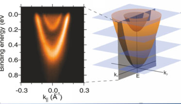
In this presentation, examples from the surface and bulk electronic properties of InN, In-rich InGaN, and several epitaxially grown oxide semiconductors, including In2O3, CdO and ZnO, will be discussed along with the effects of modifying their surfaces by controlled adsorption. The valence band density of states and the surface electronic properties of these materials have been studied using high-resolution synchrotron radiation angle-resolved photoemission (SR-ARPES) and core-level photoemission spectroscopy with hard x-rays (HAXPES), and these data are compared with theoretical DFT band structure calculations. The physical origins of this phenomenon and the quantized nature of the subsequent surface 2D electron gas, will be discussed in terms of the band structure and intrinsic properties of these materials.
Please download flyer here. All invited
Venue: G59-G60, Old Main Building K15
Address:


