- First observation of excitonic insulator
- New exotic state was first predicted in 1960s
A University of Wollongong / Monash University collaboration has found evidence of a new phase of matter predicted in the 1960s: the excitonic insulator.
The unique signatures of an excitonic insulating phase were observed in antimony Sb(110) nanoflakes.
The findings provide a novel strategy to search for more excitonic insulators which is potentially capable of carrying exciton superfluids, and further studies will be required to fully understand the rich physics of this new phase of matter.
Background
“The discovery of new phases of matter is one of the major goals of condensed matter physics and is important for developing new technologies for low energy electronics which is the main goal of the ARC center in FLEET,” says Prof Xiaolin Wang (UOW).
“In the 1960s, it was proposed that in small indirect band-gap materials, excitons can spontaneously form because the density of carriers is too low to screen the attractive Coulomb interaction between electrons and holes.” said by Dr Zhi Li, the first author and currently FLEET AI and an ARC DECRA fellow co-mentored by Prof Wang and Prof Fuhrer.
The result is a novel strongly interacting insulating phase known as an excitonic insulator.
In the insulator family, the first member is the bandgap, ‘or ‘trivial’ insulator.
Besides bandgap insulators, other insulating states may arise through the effects of electron-electron interactions or disorder coupled with quantum interference, for example:
- Anderson insulators, in which electrons are localized by quantum interference
- Topological insulators, which have a gap in the bulk but gapless conducting states at the surface/edge due to band inversion.
The excitonic insulator, a new phase of matter in the critical transition point between insulator and metal was proposed in 1960s by many pioneers in condensed matter physics.
In an excitonic insulator, bosonic particles rather than electrons determine the physical properties.
Excitonic insulators have been predicted to host many novel properties, including crystallized excitonium, superfluidity and excitonic high-temperature superconductivity, and breakthroughs in finding this new class of insulators have attracted keen attention amongst condensed matter physicists and two-dimensional material scientists.
The study
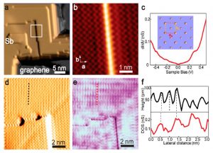
The research team employed scanning tunnelling microscopy (STM) and spectroscopy (STS) to show that the enhanced Coulomb interaction in quantum-confined elemental antimony nanoflakes drives the system to the excitonic insulator state.
The unique feature of the excitonic insulator, a charge density wave (CDW) without periodic lattice distortion, was directly observed. Furthermore, STS shows a gap induced by the CDW near the Fermi surface.
These observations suggest that the antimony (Sb(110)) nanoflake is an excitonic insulator.
“Possible Excitonic Insulating Phase in Quantum-Confined Sb Nanoflakes” was published in Nano Letters in July 2019. (DOI 10.1021/acs.nanolett.9b01123)
As well as funding by the Australian Research Council (Centre of Excellence, Future Fellowship, Discovery Projects, DECRA and LIEF funds and Laureate Fellowship), support was provided by the University of Wollongong Vice Chancellor’s Postdoctoral Research Fellowship Scheme.
The theory

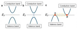
Three types of insulators. (a) Insulators with a band gap at the Fermi surface, including band insulators, Mott insulators, and Anderson insulators. (b) Topological insulators, where there are topologically protected surface states inside the band gap. (c) Excitonic insulators, where electrons and holes are bound together and form excitons at the Fermi surface.
Excitons, which are bosonic, strongly-bound pairs of electrons and holes, are formed through the attractive electron−hole Coulomb interaction, lowering the system energy by the value of the binding energy (Eb).
If such excitons could form spontaneously, then the result would be an excitonic insulator phase.
In semiconductors or insulators, the formation of an exciton requires overcoming the band-gap energy Eg needed to create an electron−hole pair. The spontaneous formation of excitons demands that Eb > Eg. However, Eg is usually much larger than Eb in semiconductors and insulators, preventing spontaneous exciton formation.
In this work, the researchers took advantage of the strong Coulomb interaction in very thin materials to promote the excitonic insulator phase in antimony.
Previous work
Up to now, many materials showing CDW have been identified as the candidate of excitonic insulators.
Unfortunately, these candidate excitonic insulators show strong periodical lattice distortion (PLD), indicating CDW was driven by electron-phonon coupling rather than by excitonic insulator states.
The new study provides solid evidence of the excitonic insulator phase in antimony nanoflakes by the observation of CDW without PLD.
Novel materials at FLEET
 The properties of novel materials are studied at FLEET, an Australian Research Council Centre of Excellence, within the Centre’s Enabling technology A.
The Centre for Future Low-Energy Electronics Technologies (FLEET) is a collaboration of over a hundred researchers, seeking to develop ultra-low energy electronics to face the challenge of energy use in computation, which already consumes 8% of global electricity, and is doubling each decade.
Each of FLEET’s three research themes are heavily enabled by these novel materials, including 2D topological materials (Research Theme 1), atomically thin semiconductors (as hosts for excitons in Research Theme 2, and for realising non-equilibrium topological phenomena in Research Theme 3).
More information
- Contact Dr Zhi Li (University of Wollongong) zhili@uow.edu.au
- Contact Prof Xiaolin Wang (University of Wollongong) xiaolin@uow.edu.au
- Contact Prof Michael Fuhrer (Monash University) michael.fuhrer@monash.edu
- Connect at @FLEETCentre
- Visit FLEET.org.au
- Read FLEET Enabling technology A: novel materials news

Charge density wave (CDW) without periodic lattice distortion (PLD) on antimony nanoflakes. (a) STM image, nanoflake. (b) STM image showing pseudosquare lattice. (c) Typical STS curve on Sb nanoflakes shows a V-shaped feature near Fermi surface, with inset showing lattice structure. (d) STM image with atomic resolution of Sb(110). (e) DOS modulation. (f) Height profile and line profile of DOS with periodic modulation.


