Surfaces on the move: dynamic liquefaction
The boundary between solid metal and liquid metal can be much less ‘solid’ than we ever suspected.
RMIT researchers have discovered that the liquid-solid boundary can fluctuate back and forth, with metallic atoms near the surface breaking free from their crystal lattice.
Observing a metal-alloy mass solidifying in a sea of liquid metal, the team was able to observe a very interesting phenomenon, never seen before: the surface metal moves from a solid state into a liquid state, and back again.
In contrast to what is known as ‘pre melting’, this phenomenon occurred at unexpectedly low temperatures, far below the melting temperature of the solid metal (eg, 200°C below liquidus).
The phenomenon also occurs to a much greater depth than anticipated within the solid metal, up to 100 atoms in depth, and was seen to continue for several days.
In addition to being an exciting new fundamental discovery about the chemistry of solid and liquid metals, there is potential application ultimately where-ever metal alloys are utilised.
Observing metals on the move
In the experimental set-up, a solid (crystalline) metal-alloy mass forms in (or ‘precipitates’ from) a surrounding ocean of liquid metal, a common process in synthesising metal alloys.
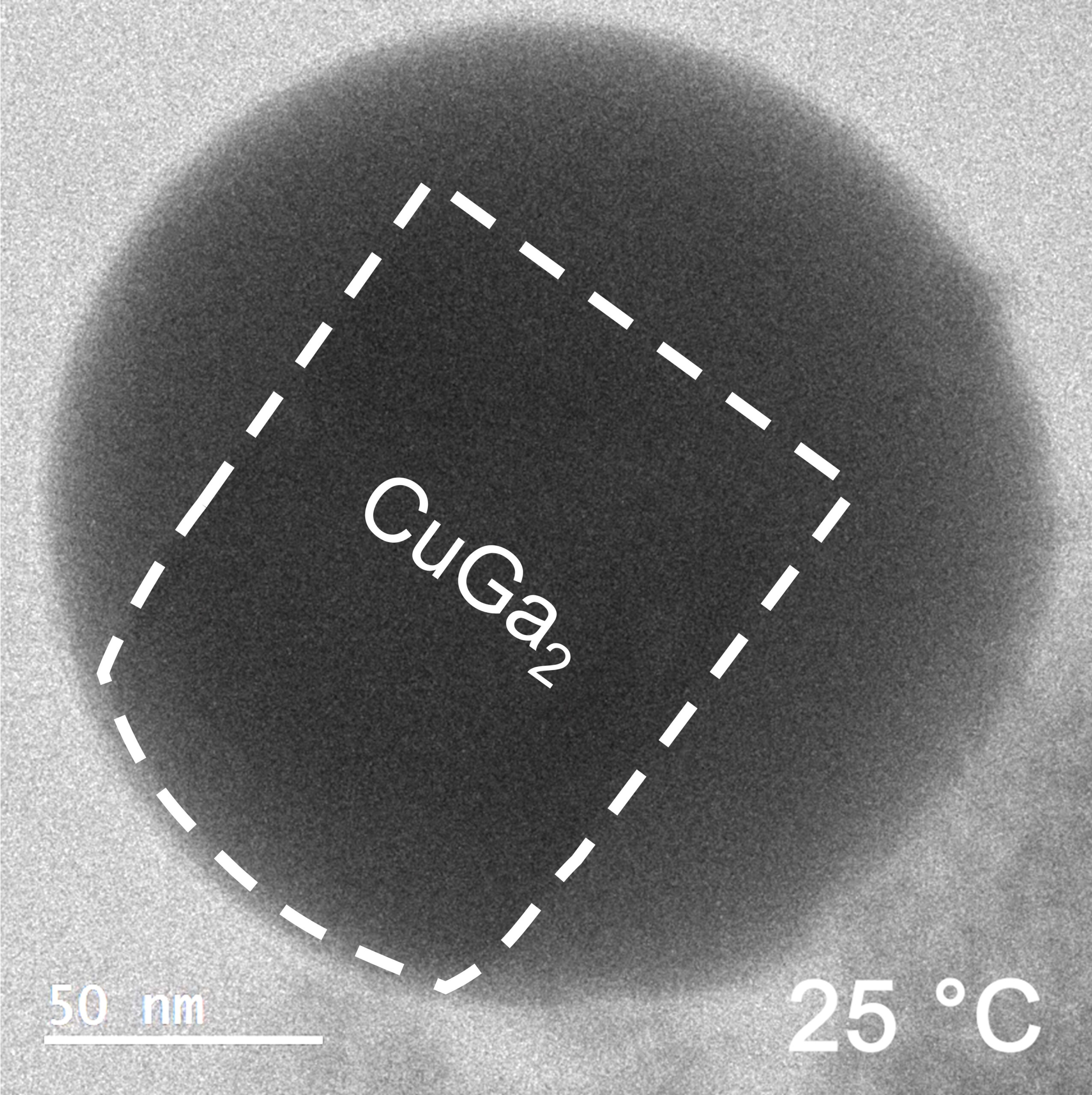
For example, a nugget of gallium-copper alloy might precipitate and grow in a sea of liquid gallium as it cools to room temperature, slightly below the melting temperature of gallium (30°C), but far below the melting temperature of the Cu-Ga alloy (256°C).
(The newly-observed fluctuating-surface phenomenon has occurred in all metal systems tested by the RMIT team, but is particularly well defined in the copper-gallium system.)
Despite the ubiquity of the liquid-metal alloying process, surprisingly little is known about the crucial surface chemistry of the process, due to the opaque nature of the liquid metal bath.
To solve this challenge, the team at RMIT directly imaged the surface phenomena of the gallium-copper mass using a Transmission Electron Microscope (TEM), which allows penetration of the liquid metal bath, and resolutions down to a nanometre scale.
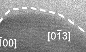
At this scale, the surface of the solid alloy can be seen to be fluctuating between solid and liquid phase, at a rate of several times per second, and to a depth of around 10 nm, or 50-100 atoms.
“This fluctuation of the solid metal surface between solid and liquid phases was completely unexpected,” says lead author Caiden Parker, “because the entire system was being kept at close to room-temperature conditions.”
“The liquid gallium ocean was over 200°C colder than the melting point of the Cu-Ga alloy. There would have seemed no possible reason for its surface to keep reverting back to liquid form,” says Caiden, who is a FLEET PhD candidate at RMIT.
In the video, the crystalline Cu-Ga alloy is identifiable from the regular lattice structure, which appears as diagonal stripes. The surrounding grey area is liquid gallium and not empty space.
Escape and recapture: A molecular view of the fluctuating boundary
“The outer layers of a solid metal alloy are surprisingly unstable when placed inside a liquid-metal environment, to the depth of several nanometres, fluctuating between crystalline and liquid states,” says team leader and corresponding author Prof Torben Daeneke (also at RMIT).
This crystal interface liquefaction, is observed at remarkably low temperatures (200°C below melting point of the solid), differentiating the observed liquefaction phenomenon from other processes such as surface pre-melting or conventional bulk melting.
The highly unstable crystal interface is observed in a variety of binary alloy systems and as such, the findings may impact the understanding of crystallisation and solidification processes in metallic systems and alloys more generally.
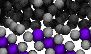
The crystal structure contains both ‘solute’ metal atoms (ie, copper) and ‘solvent’ metal atoms (gallium) thus forming a compound (CuGa2). The surface liquefaction process begins by losing some of the solvent metal atoms back into the surrounding liquid.
The researchers conducted molecular dynamic modelling in order to understand the observed surface fluidisation.
The modelling reveals that at the liquid-solid surface, some solvent (gallium) atoms will escape the solid structure due to that escape being energetically similar to staying in place.
Ie, a proportion of surface Ga atoms possess sufficient energy to escape the crystal lattice.
This ‘escape’ of atoms creates a vacancy at the surface, eventually creating an instability that leads to lattice collapse, causing the liquid-solid boundary to retreat inwards, into the solid.
Following this, the liquid becomes supersaturated in the solute (copper), forcing the surrounding liquid to re-bind with the crystal lattice. This causes the liquid-solid boundary to advance outwards again, back into the liquid.
The result is that the liquid-solid boundary oscillates backwards and forwards within a timespan of approximately half a second.
In the video of the molecular model, gallium atoms are represented in two colours: grey spheres represent gallium atoms that begin the modelled period being bound in the CuGa2 crystal lattice. Dark-grey spheres represent gallium atoms that begin the modelled period as moving freely in the surrounding liquid ocean.
The video shows a fraction of a nanosecond during the first phase of the process, when boundary shifts inwards as crystal-bound atoms escape to join the surrounding liquid.
As the model runs, grey atoms (ie, initially bound gallium atoms) escape the crystal lattice to float off into an ocean of dark grey (the surrounding liquid gallium). After a short while (a few hundred picoseconds), the purple atoms (ie, copper atoms) also begin to dislodge from the lattice.
Opportunities for further research and exciting future applications
“We hope this discovery will open new understanding of how metals behave, for creating new research opportunities, application in new alloy processes, solders, and improved additive manufacturing (3D printing) processes.
Crystallisation of alloys from a molten state is a fundamental metallurgic process, and the authors believe that the solid-liquid fluctuation of the crystal surface will be occurring every time crystallisation occurs.
“That’s why this is so exciting” says Torben. “The alloying process is so widespread, and so important in creating the materials that support modern industry….”
“Yet, no-one knew this was happening.”
“Now that we have discovered this fluctuation happening at the surface of solid alloys as they form, other metal chemistry researchers are going to want to explore this further.”
And with further improved fundamental understanding of the process of alloy crystallisation, it’s highly likely this newly discovered phenomenon will find an application.
The process of solidification in the synthesis of metal alloys is crucial, dictating the final physical, chemical and mechanical properties, all profoundly impacted by the final crystalline structure, size and shape.
“We can’t know yet what applications this might ultimately lead to,” says Caiden. “We don’t know whether someone will use this new understanding to synthesise improved alloys, or to reduce energy-use in alloy creation, or… who knows what!”
“That’s why fundamental science is so cool!”
The study
“Spontaneous Liquefaction of Solid Metal–Liquid Metal Interfaces in Colloidal Binary Alloys” was published in Advanced Science in April 2024. DOI: 10.1002/advs.202400147

Engineering a novel supersolid state using layered 2D materials

Can a solid be a superfluid? Bilayer excitons form a quantum supersolid
A collaboration of Australian and European physicists predict that layered electronic 2D semiconductors can host a curious quantum phase of matter called the supersolid.
The supersolid is a very counterintuitive phase indeed. It is made up of particles that simultaneously form a rigid crystal and yet at the same time flow without friction since all the particles belong to the same single quantum state.
A solid becomes ‘super’ when its quantum properties match the well-known quantum properties of superconductors. A supersolid simultaneously has two orders, solid and super:
- solid because of the spatially repeating pattern of particles,
- super because the particles can flow without resistance.
“Although a supersolid is rigid, it can flow like a liquid without resistance,” explains Lead author Dr Sara Conti (University of Antwerp).
The study was conducted at UNSW (Australia), University of Antwerp (Belgium) and University of Camerino (Italy).
A 50-year journey towards the exotic supersolid
Geoffrey Chester, a Professor at Cornell University, predicted in 1970 that solid helium-4 under pressure should at low temperatures display:
- Crystalline solid order, with each helium atom at a specific point in a regularly ordered lattice and, at the same time,
- Bose-Einstein condensation of the atoms, with every atom in the same single quantum state, so they flow without resistance.
However in the following five decades the Chester supersolid has not been unambiguously detected.
Alternative approaches to forming a supersolid-like state have reported supersolid-like phases in cold-atom systems in optical lattices. These are either clusters of condensates or condensates with varying density determined by the trapping geometries. These supersolid-like phases should be distinguished from the original Chester supersolid in which each single particle is localised in its place in the crystal lattice purely by the forces acting between the particles.
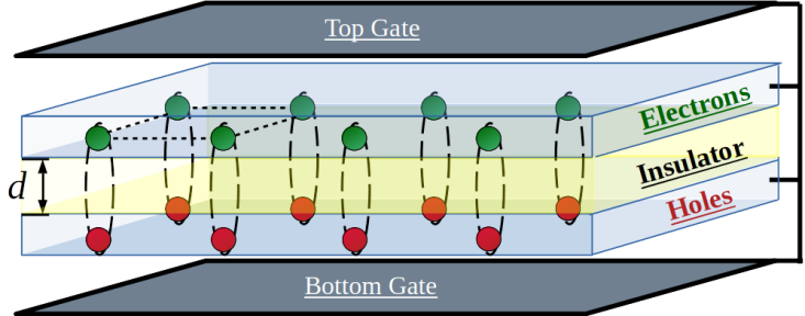
The new Australia-Europe study predicts that such a state could instead be engineered in two-dimensional (2D) electronic materials in a semiconductor structure, fabricated with two conducting layers separated by an insulating barrier of thickness d.
One layer is doped with negatively-charged electrons and the other with positively-charged holes.
The particles forming the supersolid are interlayer excitons, bound states of an electron and hole tied together by their strong electrical attraction. The insulating barrier prevents fast self-annihilation of the exciton bound pairs. Voltages applied to top and bottom metal ‘gates’ tune the average separation r0 between excitons.
The research team predicts that excitons in this structure will form a supersolid over a wide range of layer separations and average separations between the excitons. The electrical repulsion between the excitons can constrain them into a fixed crystalline lattice.
“A key novelty is that a supersolid phase with Bose-Einstein quantum coherence appears at layer separations much smaller than the separation predicted for the non-super exciton solid that is driven by the same electrical repulsion between excitons,” says co-corresponding author Prof David Neilson (University of Antwerp).
“In this way, the supersolid pre-empts the non-super exciton solid. At still larger separations, the non-super exciton solid eventually wins, and the quantum coherence collapses.”
“This is an extremely robust state, readily achievable in experimental setups,” adds co-corresponding author Prof Alex Hamilton (UNSW). “Ironically, the layer separations are relatively large and are easier to fabricate than the extremely small layer separations in such systems that have been the focus of recent experiments aimed at maximising the interlayer exciton binding energies.”
As for detection, for a superfluid it is well known that this cannot be rotated until it can host a quantum vortex, analogous to a whirlpool. But to form this vortex requires a finite amount of energy, and hence a sufficiently strong rotational force. So up to this point, the measured rotational moment of inertia (the extent to which an object resists rotational acceleration) will remain zero. In the same way, a supersolid can be identified by detecting such an anomaly in its rotational moment of inertia.
The research team has reported the complete phase diagram of this system at low temperatures.
“By changing the layer separation relative to the average exciton spacing, the strength of the exciton-exciton interactions can be tuned to stabilise either the superfluid, or the supersolid, or the normal solid,” says Dr Sara Conti.
“The existence of a triple point is also particularly intriguing. At this point, the boundaries of supersolid and normal-solid melting, and the supersolid to normal-solid transition, all cross. There should be exciting physics coming from the exotic interfaces separating these domains, for example, Josephson tunnelling between supersolid puddles embedded in a normal-background.”
The study
Chester Supersolid of Spatially Indirect Excitons in Double-Layer Semiconductor Heterostructures was published in Physical Review Letters in February 2023. (DOI 10.1103/physrevlett.130.057001)
Tiny device mimics human vision and memory abilities
Researchers have created a small device that ‘sees’ and creates memories in a similar way to humans, in a promising step towards one day having applications that can make rapid, complex decisions such as in self-driving cars.
The neuromorphic invention is a single chip enabled by a sensing element, doped indium oxide, that is thousands of times thinner than a human hair and requires no external parts to operate.
RMIT University engineers led the work, with contributions from researchers at Deakin University and the University of Melbourne.
The team’s research demonstrates a working device that captures, processes and stores visual information. With precise engineering of the doped indium oxide, the device mimics a human eye’s ability to capture light, pre-packages and transmits information like an optical nerve, and stores and classifies it in a memory system like the way our brains can.
Collectively, these functions could enable ultra-fast decision making, the team says.
Team leader Professor Sumeet Walia said the new device can perform all necessary functions – sensing, creating and processing information, and retaining memories – rather than rely on external energy-intensive computation, which prevents real-time decision making.
“Performing all of these functions on one small device had proven to be a big challenge until now,” said Walia from the School of Engineering.
“We’ve made real-time decision making a possibility with our invention, because it doesn’t need to process large amounts of irrelevant data and it’s not being slowed down by data transfer to separate processors.”
What did the team achieve and how does the technology work?

The new device was able to demonstrate an ability to retain information for longer periods of time, compared to previously reported devices, without the need for frequent electrical signals to refresh the memory. This ability significantly reduces energy consumption and enhances the device’s performance.
Their findings and analysis are published in Advanced Functional Materials.
First author and RMIT PhD researcher Aishani Mazumder said the human brain used analog processing, which allowed it to process information quickly and efficiently using minimal energy.
“By contrast, digital processing is energy and carbon intensive, and inhibits rapid information gathering and processing,” she said.
“Neuromorphic vision systems are designed to use similar analog processing to the human brain, which can greatly reduce the amount of energy needed to perform complex visual tasks compared with today’s technologies.”
What are the potential applications?
The team used ultraviolet light as part of their experiments, and are working to expand this technology even further for visible and infrared light – with many possible applications such as bionic vision, autonomous operations in dangerous environments, shelf-life assessments of food and advanced forensics.
“Imagine a self-driving car that can see and recognise objects on the road in the same way that a human driver can or being able to able to rapidly detect and track space junk. This would be possible with neuromorphic vision technology.”
Walia said neuromorphic systems could adapt to new situations over time, becoming more efficient with more experience.
“Traditional computer vision systems – which cannot be miniaturised like neuromorphic technology – are typically programmed with specific rules and can’t adapt as easily,” he said.
“Neuromorphic robots have the potential to run autonomously for long periods, in dangerous situations where workers are exposed to possible cave-ins, explosions and toxic air.”
The human eye has a single retina that captures an entire image, which is then processed by the brain to identify objects, colours and other visual features.

The team’s device mimicked the retina’s capabilities by using single-element image sensors that capture, store and process visual information on one platform, Walia said.
“The human eye is exceptionally adept at responding to changes in the surrounding environment in a faster and much more efficient way than cameras and computers currently can,” he said.
“Taking inspiration from the eye, we have been working for several years on creating a camera that possesses similar abilities, through the process of neuromorphic engineering.”
Story first published: RMIT
‘Long duration persistent photocurrent in 3 nm thin doped indium oxide for integrated light sensing and in-sensor neuromorphic computation’, was published in Advanced Functional Materials in June 2023 (DOI: 10.1002/adfm.202303641)
‘Target identified’: teaching a machine how to identify imperfections in 2D materials
Applying machine learning to automated characterisation of atomically-thin materials
Just as James Cameron’s Terminator-800 was able to discriminate between “clothes, boots, and a motorcycle”, a FLEET study demonstrates potential for machine learning to identify different areas of interest on 2D materials.
The simple, automated optical identification of fundamentally different physical areas on these materials (e.g. areas displaying doping, strain, and electronic disorder) could significantly accelerate the science of atomically-thin materials.
Atomically-thin (or 2D) materials, including metals, semiconductors, insulators, and more-exotic quantum materials such as topological insulators, superconductors and ferromagnets, are studied by scientists around the world seeking to take advantage of their unique properties.
Materials scientists have utilised this monolayer ‘zoo’ to construct next-generation, energy-efficient electronics, batteries, memory cells and photodiodes.
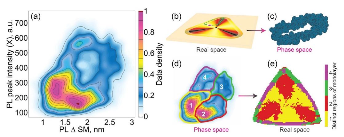
“Without any supervision, machine-learning algorithms were able to discriminate between differently perturbed areas on a 2D semiconducting material,” explains lead author Dr Pavel Kolesnichenko (Swinburne University of Technology). “This can lead to fast, machine-aided characterisation of 2D materials in the future, accelerating application of these materials in future technologies.”
However with the integration of 2D materials into next-generation technologies still involving mostly manual assembly in one-off prototypes, there is still a long way to go to reach industrial-scale production and commercialisation.
Factors that have hindered progress include lack of full control over materials fabrication, the need for experienced oversight of complex characterisation techniques, and the extreme sensitivity of monolayer materials to perturbations, many of which are introduced unintentionally.
Understanding these perturbations is a non-trivial task, as they can have a combined effect and have to be disentangled.
“So many factors can affect opto-electronic properties of 2D materials, including the type of substrate, additional doping, strain, the presence of wrinkles, defects, and environmental molecules – you name it,” says Pavel.
Pavel and Prof Jeff Davis (also at Swinburne) realised that the laborious task of 2D materials characterisation could be accomplished by machines in a rapid and automated manner.
Working with FLEET colleague Prof Michael Fuhrer (Monash University), they applied unsupervised machine-learning algorithms to characterise the semiconducting monolayer tungsten disulphide. The learning algorithms were able to discriminate between the areas on a monolayer flake affected by doping, strain, disorder, and the presence of additional layers.
This is the first time such a systematic disentanglement of these perturbations has been performed.
The team built on previous scientific results in the field including previous work at FLEET, where they disentangled perturbations using correlated photoluminescence and absorption spectra.
In the era of data-driven science and technology, the authors hope that their research will motivate the creation of a large labelled dataset, where labels (such as ‘doping’, or ‘strain’) would be assigned by experienced researchers.
This dataset would be then used to train deep neural networks to characterise 2D materials in a fraction of a second. The researchers believe that their work will help to introduce standards for characterisation of monolayer matter, approaching the moment of large-scale use of low-energy smartphones and computers in the future.
“Disentangling the effects of doping, strain and disorder in monolayer WS2 by optical spectroscopy” was published in 2D Materials in January 2020. (DOI: 10.1088/2053-1583/ab626a)
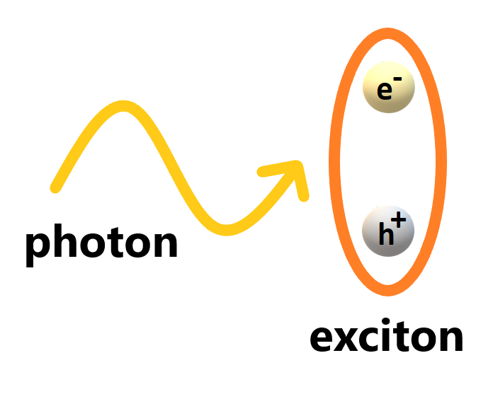
Sandwich-style construction: towards ultra-low-energy exciton electronics
New microcavity construction technique allows observation of robust, room-temperature exciton transport
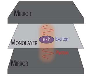
A new FLEET-led ‘sandwich-style’ fabrication process placing an atomically-thin semiconductor between two mirrors allows a significant step towards ultralow-energy electronics based on exciton-polaritons.
The breakthrough, led by PhD candidate Matthias Wurdack at ANU, demonstrated robust, dissipationless propagation of an exciton mixed with light bouncing between the high-quality mirrors.
Conventional electronics relies on flowing electrons, or holes (a hole is the absence of an electron, i.e. a positively-charged quasiparticle).
Instead, FLEET’s ANU team investigated an alternative future electronic technology using excitons because, in principle, they could flow in a semiconductor without losing energy by forming a collective superfluid state. Also, excitons in novel, actively-studied atomically-thin semiconductors are stable at room temperature. Despite this promise for low-energy electronics and sensors, the properties of
atomically-thin semiconductors, including the flow of excitons, are strongly affected by disorder or imperfections, which can be introduced during fabrication.
The ANU-led FLEET team – with Centre colleagues at Swinburne University of Technology and FLEET Partner institution Wroclaw University – coupled the excitons in an atomically-thin material to light, to demonstrate for the first time their long-range propagation without any dissipation of energy, at room temperature.
Trapping light between two parallel high-quality mirrors in an optical microcavity an exciton (matter) to bind with a photon (light), forming the hybrid particle an exciton-polariton. Microcavities are micrometre-scale structures with an optical medium sandwiched between ultra-reflective mirrors, used to confine light such that it forms exciton-polaritons.
In the 2021 study, a new ‘sandwich-style’ fabrication process for the optical microcavity allowed the researchers to minimise damage to the atomically-thin semiconductor and to maximise the interaction between the excitons and the photons. The exciton-polaritons formed in this structure were able to propagate without energy dissipation across tens of micrometres, the typical scale of an electronic microchip.
A high-quality optical microcavity ensuring the longevity of the light (photonic) component of exciton-polaritons was the key to these observations. “We found that exciton-polaritons can be made remarkably stable if microcavity construction avoids damage of the fragile semiconductor sandwiched between the mirrors during fabrication,” says Matthias.
“The choice of the atomically-thin material in which the excitons travel is far less important than the construction.”
“We fabricate the entire top structure separately, and then place it on top of the semiconductor mechanically, like making a sandwich. Thus we avoid any damage to the atomically-thin semiconductor, and preserve the properties of its excitons.”
The researchers optimised this sandwiching method to make the cavity very short, maximising the exciton-photon interaction.
“This demonstration, for the first time, of dissipationless transport of room-temperature polaritons in atomically-thin TMDCs is a significant step towards future, ultra-low-energy exciton-based electronics,” says group leader Prof Elena Ostrovskaya (ANU).
Furthermore, the researchers confirmed that exciton-polaritons can propagate in the atomically-thin semiconductor for tens of micrometres (easily far enough for functional electronics) without scattering on material defects. (In fact, the travel length of excitons in these materials is dramatically reduced by these defects.) The exciton-polaritons’ high coherence bodes well for their potential as information carriers.
“This long-range, coherent transport was achieved at room temperature, which is important for development of practical applications of atomically-thin semiconductors,” said Matthias.
If future excitonic devices are to be a viable, low-energy alternative to conventional electronic devices, they must be able to operate at room temperature, without the need for energy-intensive cooling.
Motional narrowing, ballistic transport, and trapping of room-temperature exciton polaritons in an atomically-thin semiconductor was published in Nature Communications in September 2021 (DOI: 10.1038/s41467-021-25656-7)

Beating Boltzmann’s tyranny: Surpassing lower limit on computing energy consumption
Topological insulators can reduce transistor switching energy by a factor of four, defeating ‘Boltzmann's tyranny’, which puts a lower limit on operating voltage
A landmark theoretical FLEET study in 2021 confirms the potential for topological materials to substantially reduce the energy consumed by computing, defeating Boltzmann’s tyranny, a lower limit on operating energy.
The collaboration of researchers from three FLEET nodes showed that transistors based on topological insulators rather than conventional semiconductors could reduce the gate voltage by half, and the energy used by each transistor by a factor of four.
This overcomes the famous Boltzmann’s tyranny, which puts a lower limit on transistor switching energy.
The research discovered something surprising: a gate voltage applied to a topological insulator could create a barrier to electron flow that is larger than the voltage itself times the electron charge, a result previously thought impossible.
Transistors switch on and off based on application of a gate voltage, with the energy used to charge up the gate electrode lost each time each transistor switches. With literally billions of transistors turning on and off billions of times each second, this adds up to a lot of energy.
In conventional semiconductor transistors, a gate voltage shifts the semiconductor’s ‘bandgap’ (or the range of energies within which electrons are forbidden) to allow (the ‘on’ state) or block (the ‘off’ state) incoming electrons.
In an ideal transistor, 1 volt applied to the gate would move up the range of energies blocked by 1 electron-volt. But leakage ‘tyranny’ puts a lower limit on that switching energy.
With electrons’ energies inherently ‘smeared out’, there are always a few electrons with sufficiently-high energy to make it over the barrier. This ‘leakage’ current represents wasted energy.
To avoid wasted leakage current requires a minimum gate voltage that puts a lower limit on switching energy.
Named ‘Boltzmann’s tyranny’, after the scientist who first described the ‘smearing’ of the energies of particles by temperature, this limits how small the operating gate voltage can be for a transistor, no matter what material it is made of.
However, FLEET researchers wondered whether Boltzmann’s tyranny could be overcome in a new type of transistor using topological insulators, switched via an electric field rather than gate voltage.
Two-dimensional topological insulators can function as the ‘on’ state of a new type of transistor, with current carried by the conducting edges.
The conducting state of a such a material can be changed by an electric field, switching the material from dissipationless conduction (a topological insulator with a negative bandgap) to non-conduction (effectively, functioning as a regular semiconductor, with a positive bandgap blocking electron flow).
Crucially, the team found that, unlike a regular semiconductor, the increase in the bandgap in the topological insulator could be larger than the voltage applied to the gate, beating Boltzmann’s tyranny.
The next steps will be to confirm these findings in the laboratory, using candidate materials such as bismuthene, with FLEET working to synthesise these new materials, characterise them, and incorporate them into electronic devices.
Overcoming Boltzmann’s Tyranny in a Transistor via the Topological Quantum Field Effect was published in Nano Letters in March 2021 (DOI 10.1021/acs.nanolett.1c00378)

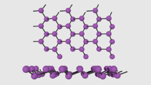
Manipulating interlayer magnetic coupling in vdW hetero-structures
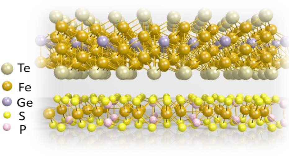
Electrical gate control in vdW heterostructures towards future spintronics
A FLEET RMIT-led international collaboration in 2022 observed, for the first time, electric gate-controlled exchange-bias effect in a van der Waals (vdW) hetero-structure, offering a promising platform for future energy-efficient, beyond-CMOS spintronics.
This new form of gate control would provide scalable, energy-efficient spin-orbit logic, which is very promising for beyond-CMOS devices in future low-energy electronic technologies.
It is the first successful significant manipulation of the exchange-bias effect (which is caused by interlayer magnetic coupling), which has been a significant goal in spintronics.
Electrical gate-manipulated exchange-bias effects in such magnetic hetero-structures enable scalable, energy-efficient spin-orbit logic, with the ‘blocking’ temperature of the exchange-bias effect effectively tuned via an electric gate.

This would allow the exchange-bias field to be turned ‘ON’ and ‘OFF’ in future spintronic transistors.
The FLEET-led collaboration of researchers at RMIT University and South China University of Technology confirmed for the first time the electric control of exchange-bias effect in a vdW heterostructure comprising antiferromagnetic (AFM) and ferromagnetic (FM) layers.
Such vdW magnetic hetero-structures provide an ideal platform for exploring interfacial magnetic-coupling mechanisms, boosting the development of vdW magnetic and spintronic devices.
The exchange-bias effect originates from the AFMFM interface coupling-induced unidirectional anisotropy. FLEET Research Fellow Dr Sultan Albarakati (RMIT)
“We decided it was time to utilise our experience in vdW hetero-structure-based nanodevices and gate control towards control magnetic properties in FM/ AFM bilayers,” says the study’s first author, FLEET Research Fellow Dr Sultan Albarakati (RMIT).
The team was also familiar with proton intercalation, which is an effective tool for modulating materials’ charge density.
The team’s expertise with magnetic materials informed materials chosen for the successful structure: a three-layer nanodevice featuring a ferromagnetic layer, antiferromagnetic layer and solid proton conductor.
The team then observed the shift of exchange-bias fields under different gate voltages.
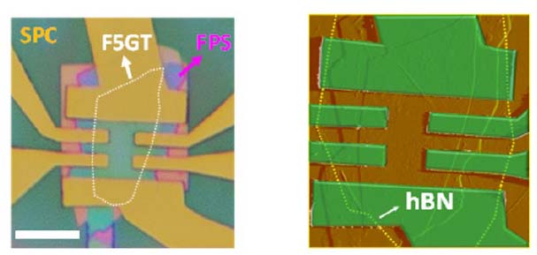
“The blocking temperature of the exchange-bias effect can be effectively tuned via an electric gate. And more interestingly, the EB field can be switched ‘ON’ and ‘OFF’ repeatably under various gate voltages,” says co-author Dr Guolin Zheng (RMIT).
“Electric Control of Exchange Bias Effect in FePS3−Fe5GeTe2 van der Waals Heterostructures” was published in Nano Letters in August 2022. (DOI: 10.1021/acs.nanolett.2c01370)

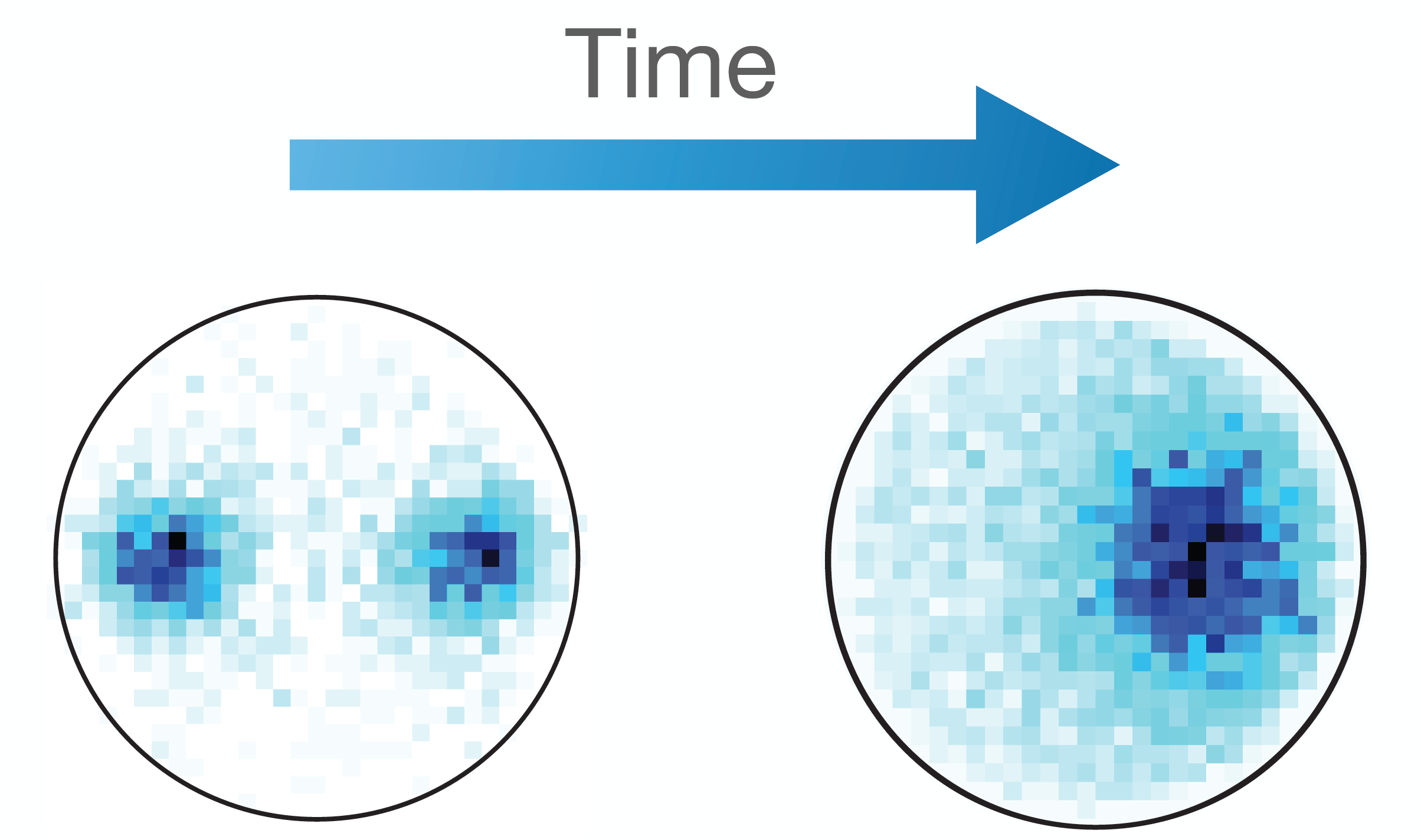
Superfluids provide new insight into turbulence
University of Queensland researchers from FLEET and a partner Centre of Excellence experimentally validated a decades’ old vortex theory, with implications for technological applications of superfluid, such as precision sensing.
Eddies in the quantum state known as a superfluid merge to form large vortices, analogous to how cyclones form in the turbulent atmosphere.
Lead author and theorist FLEET Research Fellow Dr Matt Reeves says the team’s results provide experimental validation of the 70-year-old Onsager theory – a model for two-dimensional vortex equilibrium by Nobel Laureate Lars Onsager.
“Large, long-lived vortices like cyclones or Jupiter’s Great Red Spot often form out of turbulent fluid flows, such as the atmospheres of planets,” says Matt.
Onsager’s model explains the existence of these structures, but prior to this 2022 collaborative study with the Australian Research Council Centre of Excellence for Engineered Quantum Systems (EQUS), experiments have tended to conflict with the predictions.
A key complication is that most fluids are viscous, meaning they resist flow. Superfluids, which have no viscosity, are therefore ideal candidates to realise Onsager’s model.
Cyclones, such as Jupiter’s Great Red Spot, are ‘constrained’ in the third dimension (up and down), and thus operate as 2D vortices.
The team studied the behaviour of vortices in a Bose-Einstein condensate, a type of superfluid produced by cooling a gas of rubidium atoms to extremely cold temperatures.
“We created a thin disc of the superfluid and then used lasers to inject vortices at carefully specified locations,” says EQUS researcher Dr Tyler Neely, who led the experiments.
The vortices mixed rapidly, merging into a single large cluster in only a few seconds, much like a large cyclone forming from the turbulent atmosphere.
However, the most exciting thing was the remarkable agreement between theory and experiment – the theory predicted the shape of the final giant vortex structures in the superfluid exceptionally well.
This work answers some of the key outstanding questions from previous work by the team on vortex clusters, which was published in 2019 in Science.
This article first published by ARC Centre of Excellence for Engineered Quantum Systems
Turbulent Relaxation to Equilibrium in a Two-Dimensional Quantum Vortex Gas was published in Physical Review X in February 2022 (DOI: 10.1103/PhysRevX.12.011031.

Combining irradiation and lithography to engineer advanced conductive materials
Top-down patterning of topological surface and edge states using a focused ion beam for energy-efficient quantum electronics
A new process developed to engineer nanoscale arrays of conducting channels for advanced scalable electronic circuitry unveils a useful pathway towards scalable topological electronics.
Using ion implantation and lithography, investigators created patterns of topological surface edge states on a topological material that made the surface edges conductive while the bulk layer beneath remained an insulator.
Low-energy ion implantation, neutron and X-ray reflectometry techniques at ANSTO supported the investigation, which was led by FLEET researchers at the University of Wollongong.
Investigators created patterns of topological surface edge states on antimony telluride (Sb2Te3 ), producing a 3D topological insulator with gapless, conductive surface edges and energy-gapped insulating bulk interior.
“The irradiation displaced atoms causing the transformation of the surface from a crystalline to a disordered glassy state,” explained FLEET Associate Investigator Dr David Cortie (ANSTO), who supervised lead author Abdulhakim Bake.
Ion beam implantation, commonly used to modify the properties of electronic materials by customised doping, has only recently been demonstrated on 2D materials or topological insulators.
In the work by Cortie’s team, lateral patterns were etched on thin flakes of the materials using a focused ion beam (FIB) instrument using low-energy gallium ions, such that the ions penetrate only a few nanometres into the material.
The researchers were able to combine ion beams and lithography to achieve dimensions smaller than 20 nanometres, with the shallow ion irradiation changing the surface’s atomic structure and electronic properties.
Importantly, the change in surface conductivity occurred at room temperature, suggesting a radical change in the electronic structure, confirmed by atomic force microscopy measurements by Dr Peggy Zhang, a Women in FLEET Fellow at UNSW.

X-ray diffraction and cross-sectional transmission electron microscopy confirmed the phase transition, and further experimentation with X-ray reflectometry and neutron reflectometry provided insights into the optimum ion beam dose to achieve the conversion.
Neutron reflectometry verified the thickness and morphology of the thin films and confirmed that the material remained the same chemical compound after the irradiation.
“The trick here is the judicious choice of the irradiation dose: if you under-irradiate, very little happens to the structure. But if you over-irradiate, you destroy the material via sputtering. We confirmed that we found the sweet spot for amorphisation,” said Dr Cortie.
Several different types of material were irradiated, including antimony telluride, bismuth telluride and bismuth selenide.
“In addition to standard FIB techniques, we also took advantage of the low energy implanter at ANSTO which is very flexible and can produce many different types of ions, including the noble gases and transition metal ions,” said Dr Cortie.
“The fields of amorphous and quasi-crystalline topological insulators are attracting a great deal of attention within the materials science sector. Our work provides some of the first experiments and should be useful to many people working in this field.”
“On the technological front, I also believe we have unveiled a very useful pathway towards scalable topological electronics using ion beams to define surface electronics.”
Story first published: ANSTO
Top-down patterning of topological surface and edge states using a focused ion beam was published in Nature Communications in March 2023 (DOI 10.1038/s41467-023-37102-x)

Listening to nanoscale atomic avalanches
Listening to ‘crackling’ noise of atoms shifting at nanoscale when materials are deformed towards proposed, future domain-wall electronics.
A 2023 UNSW-led FLEET study published in Nature Communications presented an exciting new way to listen to avalanches of atoms in crystals.
The nanoscale movement of atoms when materials deform leads to sound emission. This so-called crackling noise is a scale-invariant phenomenon found in various material systems as a response to external stimuli such as force or external fields.
Jerky material movements in the form of avalanches can span many orders of magnitude in size and follow universal scaling rules described by power laws. The concept was originally studied as Barkhausen noise in magnetic materials and now is used in diverse fields from earthquake research and building materials monitoring to fundamental research involving phase transitions and neural networks.
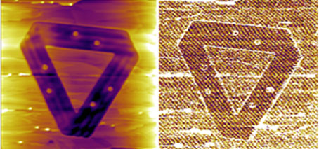
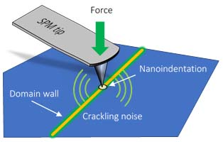
The new method for measuring nanoscale crackling noise developed by UNSW and University of Cambridge researchers is based on scanning probe microscope (SPM) nanoindentation (see figure).
“Our method allows us to study the crackling noise of individual nanoscale features in materials, such as domain walls in ferroelectrics,” says lead author Dr Cam Phu Nguyen. “The types of atom avalanches differ around these structures when the material deforms.”
One of the method’s most intriguing aspects is the fact that individual nanoscale features can be identified by imaging the material surface before indenting it. This differentiation enables new studies that were not possible previously. In a first application of the new technology, the UNSW researchers have used the method to investigate discontinuities in ordered materials, called domain walls.
“Domain walls have been the focus of our research for some time. They are highly attractive as building blocks for post–Moore’s Law electronics,” says author Prof Jan Seidel, also at UNSW. “We show that critical exponents for avalanches are altered at these nanoscale features, leading to a suppression of mixed-criticality, which is otherwise present in domains.”
From the perspective of applications and novel material functionalities, crackling noise microscopy presents a new opportunity for generating advanced knowledge about such features at the nanoscale. The study discusses experimental aspects of the method and provides a perspective on future research directions and applications.
The presented concept opens the possibility of investigating the crackling of individual nanoscale features in a wide range of other material systems.
Jerky material movements in the form of avalanches can span many orders of magnitude in size and follow universal scaling rules described by power laws. The concept was originally studied as Barkhausen noise in magnetic materials and now is used in diverse fields from earthquake research and building materials monitoring to fundamental research involving phase transitions and neural networks.
The new method for measuring nanoscale crackling noise developed by UNSW and University of Cambridge researchers is based on scanning probe microscope (SPM) nanoindentation (see figure). “Our method allows us to study the crackling noise of individual nanoscale features in materials, such as domain walls in ferroelectrics,” says lead author Dr Cam Phu Nguyen. “The types of atom avalanches differ around these structures when the material deforms.”
One of the method’s most intriguing aspects is the fact that individual nanoscale features can be identified by imaging the material surface before indenting it. This differentiation enables new studies that were not possible previously. In a first application of the new technology, the UNSW researchers have used the method to investigate discontinuities in ordered materials, called domain walls.
“Domain walls have been the focus of our research for some time. They are highly attractive as building blocks for post–Moore’s Law electronics,” says author Prof Jan Seidel, also at UNSW. “We show that critical exponents for avalanches are altered at these nanoscale features, leading to a suppression of mixed-criticality, which is otherwise present in domains.”
From the perspective of applications and novel material functionalities, crackling noise microscopy presents a new opportunity for generating advanced knowledge about such features at the nanoscale. The study discusses experimental aspects of the method and provides a perspective on future research directions and applications.
The presented concept opens the possibility of investigating the crackling of individual nanoscale features in a wide range of other material systems.
The paper Crackling noise microscopy was published in Nature Communications on 16 August 2023 (Cam-Phu Thi Nguyen, Peggy Schoenherr, Ekhard K. H. Salje, and Jan Seidel, DOI: 10.1038/s41467-023-40665-4).