Electronically-smooth nature of trisodium bismuthide makes it a viable alternative to graphene/h-BN
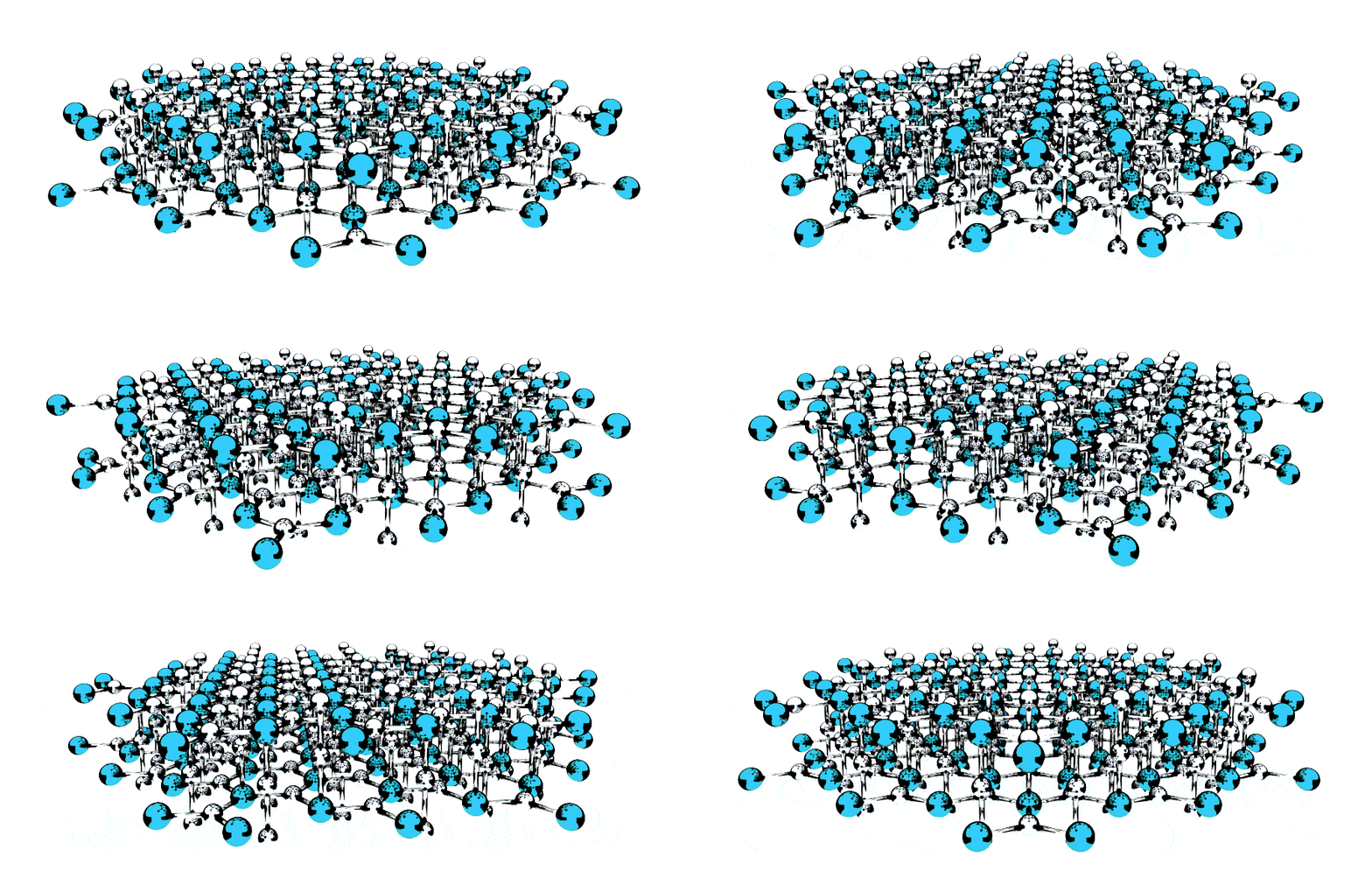
Click for animation: Trisodium bismuthide structure shown with sodium atoms white and bismuth atoms teal
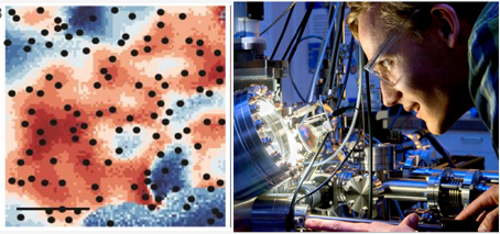
Researchers have found that the topological material trisodium bismuthide (Na3Bi) can be manufactured to be as ‘electronically smooth’ as the highest-quality graphene-based alternative, while maintaining graphene’s high electron mobility.
Na3Bi is a Topological Dirac Semimetal (TDS), considered a 3D equivalent of graphene in that it shows the same extraordinarily high electron mobility.
In graphene, as in a TDS, electrons move at constant velocity, independent of their energy.
This high electron mobility is highly desirable in materials investigated for fast-switching electronics.
The flow of electrons in graphene can be, theoretically, 100 times as fast as in silicon.
However in practice there are limitations to graphene’s remarkable electron mobility, driven by the material’s two-dimensional nature.
Although graphene itself can be extremely pure, it is far too flimsy to use as a standalone material, and must be bound with another material. And because graphene is atomically thin, impurities in that substrate are able to cause electronic disorder within the graphene.
Such microscopic inhomogeneities, known as ‘charge puddles’, limit the mobility of charge carriers.
In practice, this means that graphene-based devices must be painstakingly constructed with a graphene sheet laid upon a substrate material that minimises such electronic disorder. Hexagonal boron-nitride (h-BN) is commonly used for this purpose.
But now, researchers at Australia’s FLEET research centre have found that trisodium bismuthide (Na3Bi) grown in their labs at Monash University are as electronically smooth as the highest-quality graphene/h-BN.
It’s a significant achievement, says lead researcher Dr Mark Edmonds. “This is the first time a 3D Dirac material has been measured in such a way,” Dr Edmonds says. “And we are excited to have found such a high degree of electronic smoothness in this material.”
The discovery will be critical for advancement of the study of this new topological material, which could have wide applications in electronics. “It’s impossible to know how many fields of research this could open,” says Dr Edmonds. “The same finding in graphene/h-BN sparked considerable supplementary studies in 2011.”
With electronic-smoothness of Na3Bi now demonstrated, an array of other research possibilities open up. There have been many studies into the relativistic (high mobility) flow of electrons in graphene since it was discovered in 2004. With this latest study, similar studies into Na3Bi can be expected.
Na3Bi offers a number of interesting advantages over graphene.
As well as avoiding the difficult construction methods involved in bilayer graphene/h-BN devices, Na3Bi can be grown on a millimetre scale or larger. Currently, graphene-h-BN is limited to only a few micrometres.
Another significant advantage is the potential to use Na3Bi as the conducting channel in a new generation of transistors – one built upon the science of topological insulators.
The study was published in Science Advances in December 2017.
Next steps & topological transistors
“The discovery of electronically-smooth, thin films of TDS are an important step towards switchable topological transistors,” says FLEET Director Prof Michael Fuhrer.
“Graphene is a fantastic conductor, but it can’t be ‘switched off’, or controlled,” says Prof Fuhrer. “Topological materials, such as Na3Bi, can be switched from conventional insulator to topological insulator by the application of voltage or magnetic field.”
Topological insulators are novel materials that behave as electrical insulators in their interior, but can carry a current along their edges. Unlike a conventional electrical path, such topological edge paths can carry electrical current with near-zero dissipation of energy, meaning that topological transistors can switch without burning energy.
Topological materials were recognised in last year’s Nobel Prize in Physics.
Topological transistors would ‘switch’, just as a traditional transistor. The application of a gate potential would switch the edge paths in a Na3Bi channel between being a topological insulator (‘on’) and a conventional insulator (‘off’).
The bigger picture: energy use in computation
The overarching challenge is the growing amount of energy used in computation and information technology (IT).
Each time a transistor switches, a tiny amount of energy is burnt, and with trillions of transistors switching billions of times per second, this energy adds up. Already, the energy burnt in computation accounts for 5 per cent of global electricity use, and it’s doubling every decade.
For many years, the energy demands of an exponentially growing number of computations was kept in check by ever-more efficient, and ever-more compact computer chips – an effect related to Moore’s Law. But as fundamental physics limits are approached, Moore’s Law is ending, and there are limited future efficiencies to be found.
“For computation to continue to grow, to keep up with changing demands, we need more-efficient electronics,” says Prof Michael Fuhrer. “We need a new type of transistor that burns less energy when it switches.”
“This discovery could be a step in the direction of topological transistors that transform the world of computation.”
 About FLEET
FLEET is an Australian government-funded research centre: The Australian Research Council Centre of Excellence in Future Low-Energy Electronics Technologies.
FLEET is a collaboration of almost 100 researchers from seven Australian universities and 13 Australian and international science organisations, including the National University of Singapore, where paper co-author Shaffique Adam and others are based.
FLEET is highly interdisciplinary, with Australia’s top researchers in their fields focussing on three paths to achieve ultra-low dissipation conduction:
- Topological materials
- Exciton superfluids
- Light-transformed materials
The research, which is at the cutting edge of what’s possible in current physics, is underpinned by the science of atomically thin (two dimensional) materials and nanodevice fabrication.
Resources
• FLEET.org.au | @FLEETCentre | YouTube
Contacts
• Dr Mark Edmonds, DECRA Research Fellow FLEET, mark.edmonds@monash.edu
• Prof Michael Fuhrer, Director FLEET, michael.fuhrer@monash.edu
Images
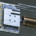
Thin film of Na3Bi grown on sapphire with gold contacts to allow for electrical measurements of the carrier density and mobility at low temperature in a magnetic field

