Some alloys are in the liquid state at or near room temperature. These alloys are usually composed of gallium and indium (elements used in low energy lamps), tin and bismuth (materials used in constructions).
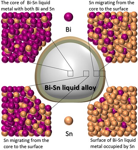
The ratio and nature of elements in liquid alloys generate extraordinary phenomena on the surface of liquid metals which have been rarely explored to date and that is competition between elements to occupy the surface of alloys. As such the composition of the surface of the alloys is different from the core and this surface area can be potentially used for harvesting novel materials with unprecedented compositions and properties.
For the first time, researchers at UNSW Sydney proposed that the phenomenon related to the surface competition between elements can be used as an approach for harvesting mixed metal oxide sheets that can be used in electronics. This observation may lead to new horizons for the production of large two-dimensional electronic materials from the surface of liquid metals for application in electronic and optic industries.
Conventionally, the fabrication processes used to manufacture electronic and optical devices are carried out in extremely clean environments under stringently controlled conditions with ultrapure materials. The smallest impurity leads to a significant loss of functionality in the final device. These processes are even more critical when the dopants are added. However, with the newly developed process, the surface enrichment and doping are naturally conducted within the alloys and contaminations by other elements are avoided.
In a new study led by CASLEO UNSW, the researchers showed the example of bismuth-tin alloys to explore the contrast between the surface and core of liquid metals. Surprisingly, in these alloys, the bismuth contents were remarkably smaller than tin in harvested nanosheets, even in very high concentrations of bismuth in the liquid alloys.
“By taking advantage of the selective enrichment of liquid metal interfaces, and harvesting the doped metal oxide semiconductor layers, the complexity of the conventional processes can be mitigated and a high degree of control over the outcomes can be achieved,” said Dr Mohammad Bagher Ghasemian, the leading author of the work.
“The idea demonstrated here offers real potential to impact several processes for the design of semiconductor materials for large scale applications in the electronics and optics industries,” added Professor Kourosh Kalantar-Zadeh, the corresponding author of this study and the director of the Centre for Advanced Solid and Liquid based Electronics and Optics (CASLEO).
Doping Process of 2D Materials Based on the Selective Migration of Dopants to the Interface of Liquid Metals was published in Advanced Materials Interfaces in September 2021. (DOI: 10.1002/adma.202104793)
The work was conducted in CASLEO at UNSW in collaboration with researchers at the University of Sydney, University of Melbourne, RMIT and ARC Centre of Excellence in Future Low-Energy Electronics Technologies (FLEET).


