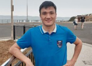
Abdulhakim Bake, UOW
The conducting boundary states of topological insulators appear at an interface where the characteristic invariant ℤ2 switches from 1 to 0. These states offer prospects for quantum electronics; however, a method is needed to spatially-control ℤ2 to pattern conducting channels. It is shown that modifying Sb2Te3 single-crystal surfaces with an ion beam switches the topological insulator into an amorphous state exhibiting negligible bulk and surface conductivity.
This is attributed to a transition from ℤ2 = 1 → ℤ2 = 0 at a threshold disorder strength. This observation is supported by density functional theory and model Hamiltonian calculations. Here we show that this ion-beam treatment allows for inverse lithography to pattern arrays of topological surfaces, edges and corners which are the building blocks of topological electronics.
About the presenter
Abdulhakim is a PhD student working with Associate Investigator David Cortie to undertake a PhD focused on magnetic materials,ion beam implantation techniques, modification of topological insulators, and device fabrication using focused ion beam microscope.
