- Oxidation of monolayer WS2 in ambient requires exposure to light, and keeping samples in darkness can protect from oxidation
- Routine exposure to room lights (days) or light microscopes can cause significant oxidation, suggesting wide reaching implications for current and future studies of monolayer S-TMDs

“This work should guide researchers in best practices for S-TMD device manufacture” Monash School of Physics and Astronomy PhD student Jimmy Kotsakidis
To protect monolayer semiconductor transition metal dichalcogenides (S-TMDs) from oxidation, they must be entirely shielded from light, with even short exposure causing oxidation severe enough to damage electrical contacts and completely destroy optical characteristics.
A new, Monash University-led collaboration has shown that the oxidation of monolayers of tungsten disulphide (WS2) in ambient conditions is due to the absorption of visible wavelengths of light.
The new work, in collaboration with researchers from the US. Naval Research Laboratory and the University of Autonomous University of Madrid, informs researchers working in the field to the heretofore unappreciated photo-sensitive nature of these materials, and more importantly, acts as a guide for completely avoiding oxidation in samples exposed to ambient conditions.
“This work should guide researchers in best practices for S-TMD device manufacture,” says lead author, Mr. Jimmy Kotsakidis.
While oxidation of monolayer semiconductor transition metal dichalcogenides (S-TMDs) in ambient conditions is already known to occur, the mechanism behind it has not been clear.
The new study shows for the first time that the oxidation of the S-TMD WS2 in ambient conditions requires light of suitable wavelength: oxidation is caused by light energetic enough to cause electronic transitions in the WS2 – that is, the observed oxidation in ambient conditions is photoinduced. The researchers postulate that this happens via two plausible mechanisms, Förster resonance energy transfer (FRET) and photo-catalysis. Due to the similar chemistry of S-TMDs, it is thought that this same effect should be observable in MoS2 and other S-TMDs in the same materials family.
Light wavelengths at 660 nm or below (i.e., visible wavelengths) was found to significantly oxidise WS2. In contrast, samples did not oxidise if exposed to 760 nm light (with too little photon energy to excite electronic transitions in WS2), or were stored in darkness (10 months), or in a light-illuminated nitrogen atmosphere (7 days).
“This important effect [photooxidation] has been overlooked in S-TMDs since oxidation studies began in circa 1955. Thus, we believe that these new findings will have significant implications for prior, present, and future studies concerning S-TMDs measured, stored, or manipulated in ambient conditions,” Mr Kotsakidis says.
Background
Atomically-thin transition metal dichalcogenides such as WS2, have garnered much interest over the past decade due to their extraordinary optical and electrical properties and thus, possible use in future electronic and optoelectronic devices.
This new work informs researchers working in the field to the heretofore unappreciated photo-sensitive nature of these materials, and more importantly, acts as a guide for completely avoiding oxidation in samples exposed to ambient conditions. While past studies have found that monolayer S-TMDs may take weeks to visibly oxidise, this work shows that this may happen in as little as 7 days even in ultra-low light conditions.
“Understanding S-TMDs’ stability in ambient conditions and under light illumination, crucial for measurements and manipulations undertaken in those conditions, is essential for their development into potential applications,” says co-author Prof Michael Fuhrer.
Method

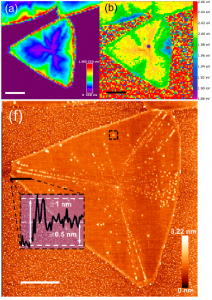
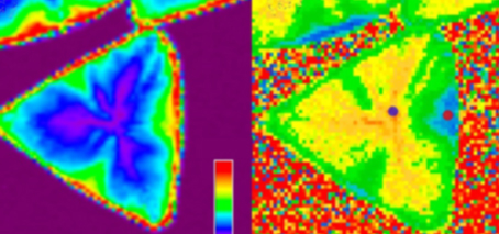
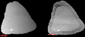
Top: three-fold symmetric, red-shifted, bright crystal edges in monolayer tungsten disulphide (WS2): (a) photoluminescent intensity map and (b) photoluminescent peak position. Bottom: The same crystal after oxidation, showing the oxide following these symmetric patterns.
The researchers studied monolayers of the semiconducting transition metal dichalcogenide (S-TMD) WS2 grown by chemical vapour deposition (CVD). The samples were exposed to controlled amounts of light, and then characterised using optical microscopy, laser scanning confocal microscopy (LSCM), photoluminescence (PL) spectroscopy, and atomic force microscopy (AFM).
The researchers found that monolayer WS2 exposed to ambient conditions in the presence of ambient light exhibited damage due to oxidation which could be detected with the LSCM and AFM, though was not evident in conventional optical microscopy due to poorer contrast and resolution.
The study observed that this oxidation was not random and was correlated with ‘high-symmetry’, high-intensity edges and red-shifted areas in the PL spectroscopy map – areas thought to contain a higher concentration of sulfur vacancies.
In contrast, samples kept in darkness showed no signs of oxidation for up to 10 months.
The researchers then performed controlled exposures to very low irradiance light at different wavelengths for long periods of time. The low intensity insured that any damage was not due to heating from the light. They found that samples exposed to light with enough photon energy to excite WS2 showed oxidation, while photon energies below this threshold did not oxidise WS2. This strong wavelength dependence and apparent lack of irradiance dependence suggests that ambient oxidation of WS2 is initiated by photon-mediated electronic band transitions, that is, photo-oxidation.
The study
Oxidation of monolayer WS2 in ambient Is a photoinduced process was published in Nano Letters on the 9th of July 2019. (DOI 10.1021/acs.nanolett.9b01599)
Initial investigations were performed at the U.S. Naval Research Laboratory (NRL). Subsequently, measurements were performed at the Melbourne Centre for Nanofabrication (MCN) in the Victorian Node of the Australian National Fabrication Facility (ANFF).
More information: Contact Jimmy C. Kotsakidis (Monash University) jckot1@student.monash.edu


