A Meet FLEET innovation-and-industry event poster

Yonatan Ashlea Alava, FLEET Research Fellow UNSW

Alex Hamilton, FLEET Deputy Director and Chief Investigator, UNSW
The Challenge

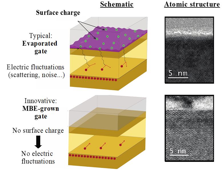
Figure 1: Unlike a typical electronic device (structure shown top left), with a rough semiconductor-oxide interface (TEM image, top right), the gate that is grown in-chamber (bottom left) displays a smooth interface, which reduces surface charge and resulting electric fluctuation.
Increasingly smaller structures in nanoelectronic devices are desirable from an industry standpoint. Smaller devices lead to increased operation speed, packing density and lower power usage.
There is a problem however with making smaller devices; the electrons need to be closer to the surface, and this worsens the electric properties of the device – such as electronic noise. This worsening occurs due to unwanted charge trapped at the surface of the device, which arises from native oxide layers that form when the substrate is taken out of the semiconductor growth chamber.
The Solution
Our solution is to fabricate the electronic device fully in the growth chamber to prevent native oxides from forming, therefore minimising surface charge.
Key Benefits
- Patented semiconductor growth technology
- Demonstrated the reduction of surface charge
- Enhanced electronic properties such as electron conductivity and ultra-low charge noise in quantum devices.
Development Stage
- Technology seeking applications
- Seeking strategic technology and partners
Brief Description & Differentiation

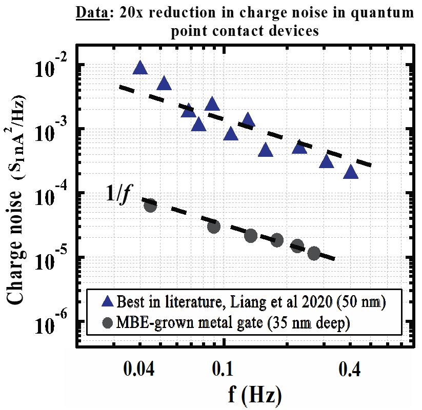
Figure 2: The new technology reduces charge noise by a factor of 20x, when compared against best-practice existing technologies.
Metal gates are necessary to control the electrical properties of electronic devices and are typically fabricated once the semiconductor is taken out of the growth chamber, leading to the formation of a native oxide at the surface.
The innovative technology used here allows the fabrication of metallic gates in the growth chamber and successfully prevents the formation of oxides and therefore surface charge, dramatically improving electrical properties such as charge noise in highly sensitive quantum devices compared to previous work (see the graph in Figure 2).
Intellectual Property
No patent
Key Publications
- High electron mobility and low noise quantum point contacts in an ultra-shallow all-epitaxial metal gate GaAs/AlxGa1−xAs heterostructure Appl. Phys. Lett. 119, 063105 (2021); DOI: 10.1063/5.0053816
More information
- Contact Prof Alex R. Hamilton UNSW alex.hamilton@unsw.edu.au
- Contact Dr Yonatan Ashlea Alava, UNSW y.ashleaalava@unsw.edu.au

