Surfaces on the move: dynamic liquefaction
The boundary between solid metal and liquid metal can be much less ‘solid’ than we ever suspected.
RMIT researchers have discovered that the liquid-solid boundary can fluctuate back and forth, with metallic atoms near the surface breaking free from their crystal lattice.
Observing a metal-alloy mass solidifying in a sea of liquid metal, the team was able to observe a very interesting phenomenon, never seen before: the surface metal moves from a solid state into a liquid state, and back again.
In contrast to what is known as ‘pre melting’, this phenomenon occurred at unexpectedly low temperatures, far below the melting temperature of the solid metal (eg, 200°C below liquidus).
The phenomenon also occurs to a much greater depth than anticipated within the solid metal, up to 100 atoms in depth, and was seen to continue for several days.
In addition to being an exciting new fundamental discovery about the chemistry of solid and liquid metals, there is potential application ultimately where-ever metal alloys are utilised.
Observing metals on the move
In the experimental set-up, a solid (crystalline) metal-alloy mass forms in (or ‘precipitates’ from) a surrounding ocean of liquid metal, a common process in synthesising metal alloys.
For example, a nugget of gallium-copper alloy might precipitate and grow in a sea of liquid gallium as it cools to room temperature, slightly below the melting temperature of gallium (30°C), but far below the melting temperature of the Cu-Ga alloy (256°C).
(The newly-observed fluctuating-surface phenomenon has occurred in all metal systems tested by the RMIT team, but is particularly well defined in the copper-gallium system.)
Despite the ubiquity of the liquid-metal alloying process, surprisingly little is known about the crucial surface chemistry of the process, due to the opaque nature of the liquid metal bath.
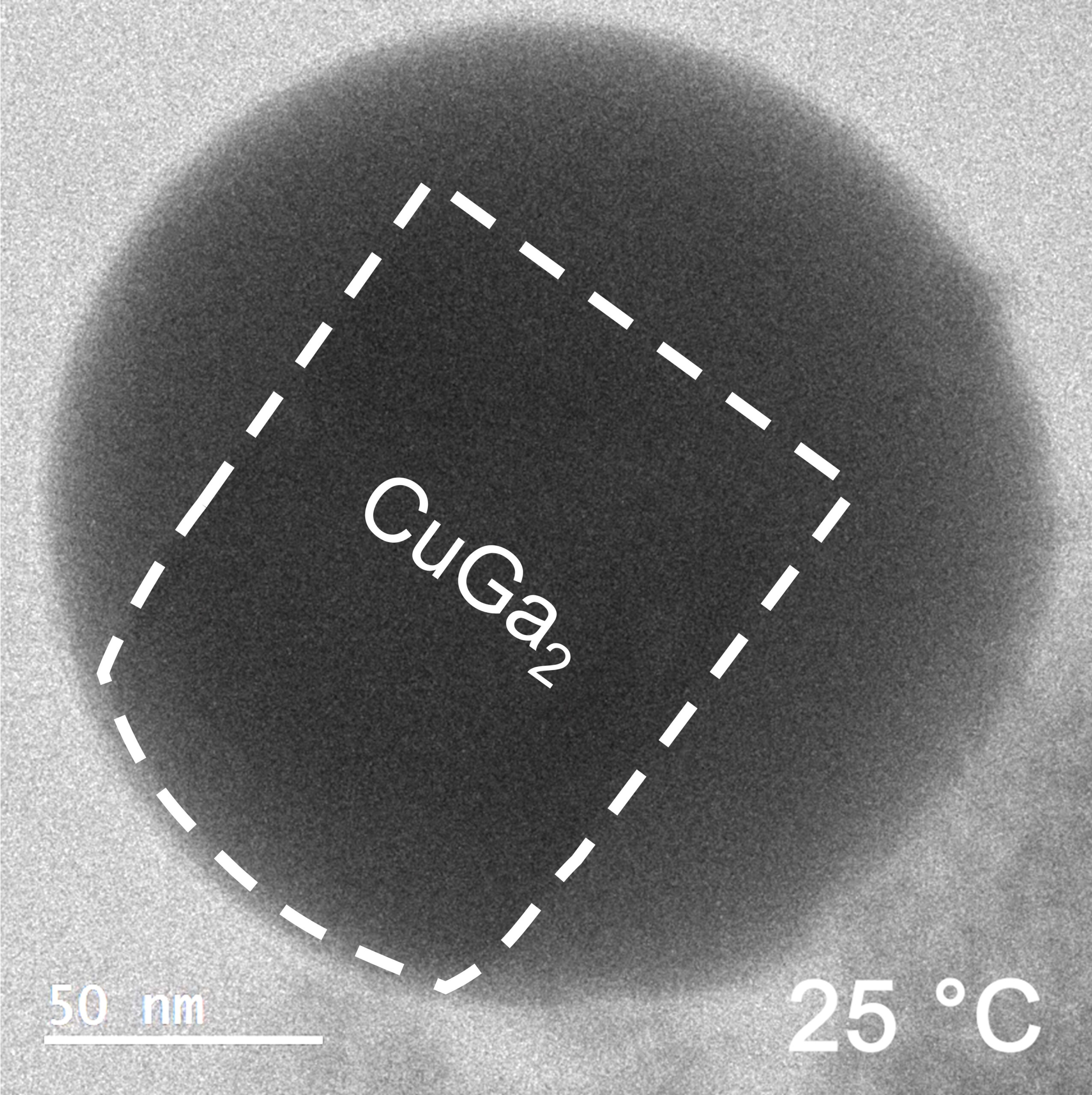
To solve this challenge, the team at RMIT directly imaged the surface phenomena of the gallium-copper mass using a Transmission Electron Microscope (TEM), which allows penetration of the liquid metal bath, and resolutions down to a nanometre scale.
At this scale, the surface of the solid alloy can be seen to be fluctuating between solid and liquid phase, at a rate of several times per second, and to a depth of around 10 nm, or 50-100 atoms.
“This fluctuation of the solid metal surface between solid and liquid phases was completely unexpected,” says lead author Caiden Parker, “because the entire system was being kept at close to room-temperature conditions.”
“The liquid gallium ocean was over 200°C colder than the melting point of the Cu-Ga alloy. There would have seemed no possible reason for its surface to keep reverting back to liquid form,” says Caiden, who is a FLEET PhD candidate at RMIT.
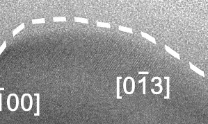
In the video, the crystalline Cu-Ga alloy is identifiable from the regular lattice structure, which appears as diagonal stripes. The surrounding grey area is liquid gallium and not empty space.
Escape and recapture: A molecular view of the fluctuating boundary
“The outer layers of a solid metal alloy are surprisingly unstable when placed inside a liquid-metal environment, to the depth of several nanometres, fluctuating between crystalline and liquid states,” says team leader and corresponding author Prof Torben Daeneke (also at RMIT).
This crystal interface liquefaction, is observed at remarkably low temperatures (200°C below melting point of the solid), differentiating the observed liquefaction phenomenon from other processes such as surface pre-melting or conventional bulk melting.
The highly unstable crystal interface is observed in a variety of binary alloy systems and as such, the findings may impact the understanding of crystallisation and solidification processes in metallic systems and alloys more generally.
The crystal structure contains both ‘solute’ metal atoms (ie, copper) and ‘solvent’ metal atoms (gallium) thus forming a compound (CuGa2). The surface liquefaction process begins by losing some of the solvent metal atoms back into the surrounding liquid.
The researchers conducted molecular dynamic modelling in order to understand the observed surface fluidisation.
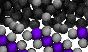
The modelling reveals that at the liquid-solid surface, some solvent (gallium) atoms will escape the solid structure due to that escape being energetically similar to staying in place.
Ie, a proportion of surface Ga atoms possess sufficient energy to escape the crystal lattice.
This ‘escape’ of atoms creates a vacancy at the surface, eventually creating an instability that leads to lattice collapse, causing the liquid-solid boundary to retreat inwards, into the solid.
Following this, the liquid becomes supersaturated in the solute (copper), forcing the surrounding liquid to re-bind with the crystal lattice. This causes the liquid-solid boundary to advance outwards again, back into the liquid.
The result is that the liquid-solid boundary oscillates backwards and forwards within a timespan of approximately half a second.
In the video of the molecular model, gallium atoms are represented in two colours: grey spheres represent gallium atoms that begin the modelled period being bound in the CuGa2 crystal lattice. Dark-grey spheres represent gallium atoms that begin the modelled period as moving freely in the surrounding liquid ocean.
The video shows a fraction of a nanosecond during the first phase of the process, when boundary shifts inwards as crystal-bound atoms escape to join the surrounding liquid.
As the model runs, grey atoms (ie, initially bound gallium atoms) escape the crystal lattice to float off into an ocean of dark grey (the surrounding liquid gallium). After a short while (a few hundred picoseconds), the purple atoms (ie, copper atoms) also begin to dislodge from the lattice.
Opportunities for further research and exciting future applications
“We hope this discovery will open new understanding of how metals behave, for creating new research opportunities, application in new alloy processes, solders, and improved additive manufacturing (3D printing) processes.
Crystallisation of alloys from a molten state is a fundamental metallurgic process, and the authors believe that the solid-liquid fluctuation of the crystal surface will be occurring every time crystallisation occurs.
“That’s why this is so exciting” says Torben. “The alloying process is so widespread, and so important in creating the materials that support modern industry….”
“Yet, no-one knew this was happening.”
“Now that we have discovered this fluctuation happening at the surface of solid alloys as they form, other metal chemistry researchers are going to want to explore this further.”
And with further improved fundamental understanding of the process of alloy crystallisation, it’s highly likely this newly discovered phenomenon will find an application.
The process of solidification in the synthesis of metal alloys is crucial, dictating the final physical, chemical and mechanical properties, all profoundly impacted by the final crystalline structure, size and shape.
“We can’t know yet what applications this might ultimately lead to,” says Caiden. “We don’t know whether someone will use this new understanding to synthesise improved alloys, or to reduce energy-use in alloy creation, or… who knows what!”
“That’s why fundamental science is so cool!”
The study
“Spontaneous Liquefaction of Solid Metal–Liquid Metal Interfaces in Colloidal Binary Alloys” was published in Advanced Science in April 2024. DOI: 10.1002/advs.202400147
‘Target identified’: teaching a machine how to identify imperfections in 2D materials
Applying machine learning to automated characterisation of atomically-thin materials
Just as James Cameron’s Terminator-800 was able to discriminate between “clothes, boots, and a motorcycle”, a FLEET study demonstrates potential for machine learning to identify different areas of interest on 2D materials.
The simple, automated optical identification of fundamentally different physical areas on these materials (e.g. areas displaying doping, strain, and electronic disorder) could significantly accelerate the science of atomically-thin materials.
Atomically-thin (or 2D) materials, including metals, semiconductors, insulators, and more-exotic quantum materials such as topological insulators, superconductors and ferromagnets, are studied by scientists around the world seeking to take advantage of their unique properties.
Materials scientists have utilised this monolayer ‘zoo’ to construct next-generation, energy-efficient electronics, batteries, memory cells and photodiodes.
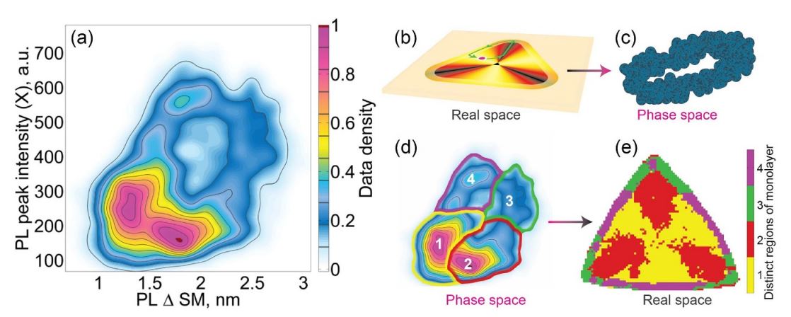
“Without any supervision, machine-learning algorithms were able to discriminate between differently perturbed areas on a 2D semiconducting material,” explains lead author Dr Pavel Kolesnichenko (Swinburne University of Technology). “This can lead to fast, machine-aided characterisation of 2D materials in the future, accelerating application of these materials in future technologies.”
However with the integration of 2D materials into next-generation technologies still involving mostly manual assembly in one-off prototypes, there is still a long way to go to reach industrial-scale production and commercialisation.
Factors that have hindered progress include lack of full control over materials fabrication, the need for experienced oversight of complex characterisation techniques, and the extreme sensitivity of monolayer materials to perturbations, many of which are introduced unintentionally.
Understanding these perturbations is a non-trivial task, as they can have a combined effect and have to be disentangled.
“So many factors can affect opto-electronic properties of 2D materials, including the type of substrate, additional doping, strain, the presence of wrinkles, defects, and environmental molecules – you name it,” says Pavel.
Pavel and Prof Jeff Davis (also at Swinburne) realised that the laborious task of 2D materials characterisation could be accomplished by machines in a rapid and automated manner.
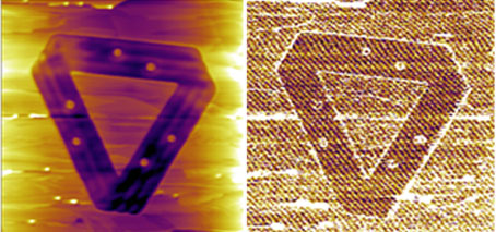
Working with FLEET colleague Prof Michael Fuhrer (Monash University), they applied unsupervised machine-learning algorithms to characterise the semiconducting monolayer tungsten disulphide. The learning algorithms were able to discriminate between the areas on a monolayer flake affected by doping, strain, disorder, and the presence of additional layers.
This is the first time such a systematic disentanglement of these perturbations has been performed.
The team built on previous scientific results in the field including previous work at FLEET, where they disentangled perturbations using correlated photoluminescence and absorption spectra.
In the era of data-driven science and technology, the authors hope that their research will motivate the creation of a large labelled dataset, where labels (such as ‘doping’, or ‘strain’) would be assigned by experienced researchers.
This dataset would be then used to train deep neural networks to characterise 2D materials in a fraction of a second. The researchers believe that their work will help to introduce standards for characterisation of monolayer matter, approaching the moment of large-scale use of low-energy smartphones and computers in the future.
“Disentangling the effects of doping, strain and disorder in monolayer WS2 by optical spectroscopy” was published in 2D Materials in January 2020. (DOI: 10.1088/2053-1583/ab626a)

Combining irradiation and lithography to engineer advanced conductive materials
Top-down patterning of topological surface and edge states using a focused ion beam for energy-efficient quantum electronics
A new process developed to engineer nanoscale arrays of conducting channels for advanced scalable electronic circuitry unveils a useful pathway towards scalable topological electronics.
Using ion implantation and lithography, investigators created patterns of topological surface edge states on a topological material that made the surface edges conductive while the bulk layer beneath remained an insulator.
Low-energy ion implantation, neutron and X-ray reflectometry techniques at ANSTO supported the investigation, which was led by FLEET researchers at the University of Wollongong.
Investigators created patterns of topological surface edge states on antimony telluride (Sb2Te3 ), producing a 3D topological insulator with gapless, conductive surface edges and energy-gapped insulating bulk interior.
“The irradiation displaced atoms causing the transformation of the surface from a crystalline to a disordered glassy state,” explained FLEET Associate Investigator Dr David Cortie (ANSTO), who supervised lead author Abdulhakim Bake.
Ion beam implantation, commonly used to modify the properties of electronic materials by customised doping, has only recently been demonstrated on 2D materials or topological insulators.
In the work by Cortie’s team, lateral patterns were etched on thin flakes of the materials using a focused ion beam (FIB) instrument using low-energy gallium ions, such that the ions penetrate only a few nanometres into the material.
The researchers were able to combine ion beams and lithography to achieve dimensions smaller than 20 nanometres, with the shallow ion irradiation changing the surface’s atomic structure and electronic properties.
Importantly, the change in surface conductivity occurred at room temperature, suggesting a radical change in the electronic structure, confirmed by atomic force microscopy measurements by Dr Peggy Zhang, a Women in FLEET Fellow at UNSW.

X-ray diffraction and cross-sectional transmission electron microscopy confirmed the phase transition, and further experimentation with X-ray reflectometry and neutron reflectometry provided insights into the optimum ion beam dose to achieve the conversion.
Neutron reflectometry verified the thickness and morphology of the thin films and confirmed that the material remained the same chemical compound after the irradiation.
“The trick here is the judicious choice of the irradiation dose: if you under-irradiate, very little happens to the structure. But if you over-irradiate, you destroy the material via sputtering. We confirmed that we found the sweet spot for amorphisation,” said Dr Cortie.
Several different types of material were irradiated, including antimony telluride, bismuth telluride and bismuth selenide.
“In addition to standard FIB techniques, we also took advantage of the low energy implanter at ANSTO which is very flexible and can produce many different types of ions, including the noble gases and transition metal ions,” said Dr Cortie.
“The fields of amorphous and quasi-crystalline topological insulators are attracting a great deal of attention within the materials science sector. Our work provides some of the first experiments and should be useful to many people working in this field.”
“On the technological front, I also believe we have unveiled a very useful pathway towards scalable topological electronics using ion beams to define surface electronics.”
Story first published: ANSTO
Top-down patterning of topological surface and edge states using a focused ion beam was published in Nature Communications in March 2023 (DOI 10.1038/s41467-023-37102-x)

Listening to nanoscale atomic avalanches
Listening to ‘crackling’ noise of atoms shifting at nanoscale when materials are deformed towards proposed, future domain-wall electronics.
A 2023 UNSW-led FLEET study published in Nature Communications presented an exciting new way to listen to avalanches of atoms in crystals.
The nanoscale movement of atoms when materials deform leads to sound emission. This so-called crackling noise is a scale-invariant phenomenon found in various material systems as a response to external stimuli such as force or external fields.
Jerky material movements in the form of avalanches can span many orders of magnitude in size and follow universal scaling rules described by power laws. The concept was originally studied as Barkhausen noise in magnetic materials and now is used in diverse fields from earthquake research and building materials monitoring to fundamental research involving phase transitions and neural networks.
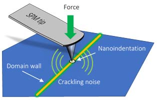
The new method for measuring nanoscale crackling noise developed by UNSW and University of Cambridge researchers is based on scanning probe microscope (SPM) nanoindentation (see figure).
“Our method allows us to study the crackling noise of individual nanoscale features in materials, such as domain walls in ferroelectrics,” says lead author Dr Cam Phu Nguyen. “The types of atom avalanches differ around these structures when the material deforms.”
One of the method’s most intriguing aspects is the fact that individual nanoscale features can be identified by imaging the material surface before indenting it. This differentiation enables new studies that were not possible previously. In a first application of the new technology, the UNSW researchers have used the method to investigate discontinuities in ordered materials, called domain walls.
“Domain walls have been the focus of our research for some time. They are highly attractive as building blocks for post–Moore’s Law electronics,” says author Prof Jan Seidel, also at UNSW. “We show that critical exponents for avalanches are altered at these nanoscale features, leading to a suppression of mixed-criticality, which is otherwise present in domains.”
From the perspective of applications and novel material functionalities, crackling noise microscopy presents a new opportunity for generating advanced knowledge about such features at the nanoscale. The study discusses experimental aspects of the method and provides a perspective on future research directions and applications.
The presented concept opens the possibility of investigating the crackling of individual nanoscale features in a wide range of other material systems.
Jerky material movements in the form of avalanches can span many orders of magnitude in size and follow universal scaling rules described by power laws. The concept was originally studied as Barkhausen noise in magnetic materials and now is used in diverse fields from earthquake research and building materials monitoring to fundamental research involving phase transitions and neural networks.
The new method for measuring nanoscale crackling noise developed by UNSW and University of Cambridge researchers is based on scanning probe microscope (SPM) nanoindentation (see figure). “Our method allows us to study the crackling noise of individual nanoscale features in materials, such as domain walls in ferroelectrics,” says lead author Dr Cam Phu Nguyen. “The types of atom avalanches differ around these structures when the material deforms.”
One of the method’s most intriguing aspects is the fact that individual nanoscale features can be identified by imaging the material surface before indenting it. This differentiation enables new studies that were not possible previously. In a first application of the new technology, the UNSW researchers have used the method to investigate discontinuities in ordered materials, called domain walls.
“Domain walls have been the focus of our research for some time. They are highly attractive as building blocks for post–Moore’s Law electronics,” says author Prof Jan Seidel, also at UNSW. “We show that critical exponents for avalanches are altered at these nanoscale features, leading to a suppression of mixed-criticality, which is otherwise present in domains.”
From the perspective of applications and novel material functionalities, crackling noise microscopy presents a new opportunity for generating advanced knowledge about such features at the nanoscale. The study discusses experimental aspects of the method and provides a perspective on future research directions and applications.
The presented concept opens the possibility of investigating the crackling of individual nanoscale features in a wide range of other material systems.
The paper Crackling noise microscopy was published in Nature Communications on 16 August 2023 (Cam-Phu Thi Nguyen, Peggy Schoenherr, Ekhard K. H. Salje, and Jan Seidel, DOI: 10.1038/s41467-023-40665-4).