Surfaces on the move: dynamic liquefaction
The boundary between solid metal and liquid metal can be much less ‘solid’ than we ever suspected.
RMIT researchers have discovered that the liquid-solid boundary can fluctuate back and forth, with metallic atoms near the surface breaking free from their crystal lattice.
Observing a metal-alloy mass solidifying in a sea of liquid metal, the team was able to observe a very interesting phenomenon, never seen before: the surface metal moves from a solid state into a liquid state, and back again.
In contrast to what is known as ‘pre melting’, this phenomenon occurred at unexpectedly low temperatures, far below the melting temperature of the solid metal (eg, 200°C below liquidus).
The phenomenon also occurs to a much greater depth than anticipated within the solid metal, up to 100 atoms in depth, and was seen to continue for several days.
In addition to being an exciting new fundamental discovery about the chemistry of solid and liquid metals, there is potential application ultimately where-ever metal alloys are utilised.
Observing metals on the move
In the experimental set-up, a solid (crystalline) metal-alloy mass forms in (or ‘precipitates’ from) a surrounding ocean of liquid metal, a common process in synthesising metal alloys.
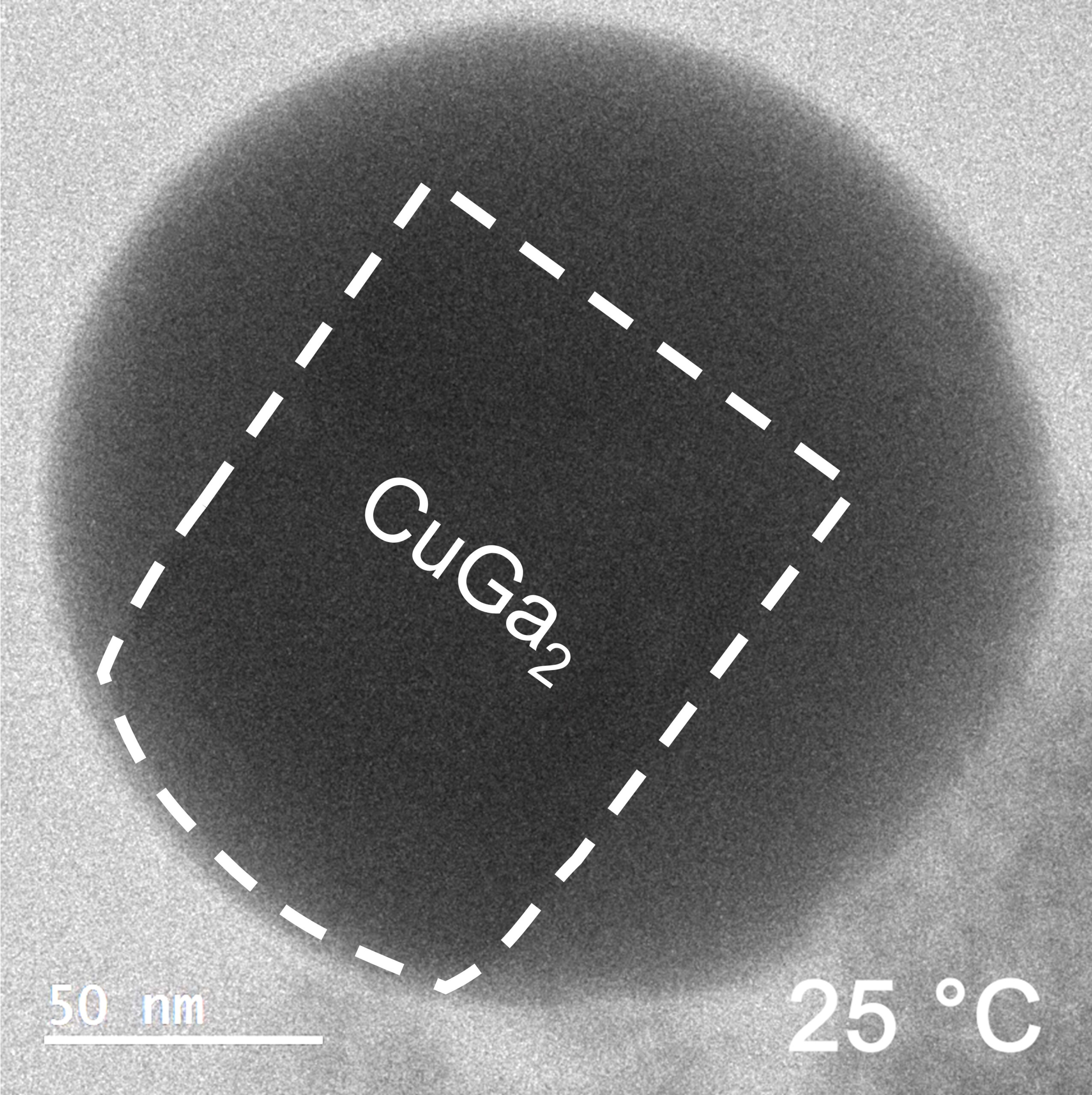
For example, a nugget of gallium-copper alloy might precipitate and grow in a sea of liquid gallium as it cools to room temperature, slightly below the melting temperature of gallium (30°C), but far below the melting temperature of the Cu-Ga alloy (256°C).
(The newly-observed fluctuating-surface phenomenon has occurred in all metal systems tested by the RMIT team, but is particularly well defined in the copper-gallium system.)
Despite the ubiquity of the liquid-metal alloying process, surprisingly little is known about the crucial surface chemistry of the process, due to the opaque nature of the liquid metal bath.
To solve this challenge, the team at RMIT directly imaged the surface phenomena of the gallium-copper mass using a Transmission Electron Microscope (TEM), which allows penetration of the liquid metal bath, and resolutions down to a nanometre scale.
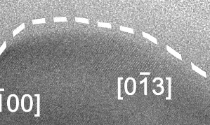
At this scale, the surface of the solid alloy can be seen to be fluctuating between solid and liquid phase, at a rate of several times per second, and to a depth of around 10 nm, or 50-100 atoms.
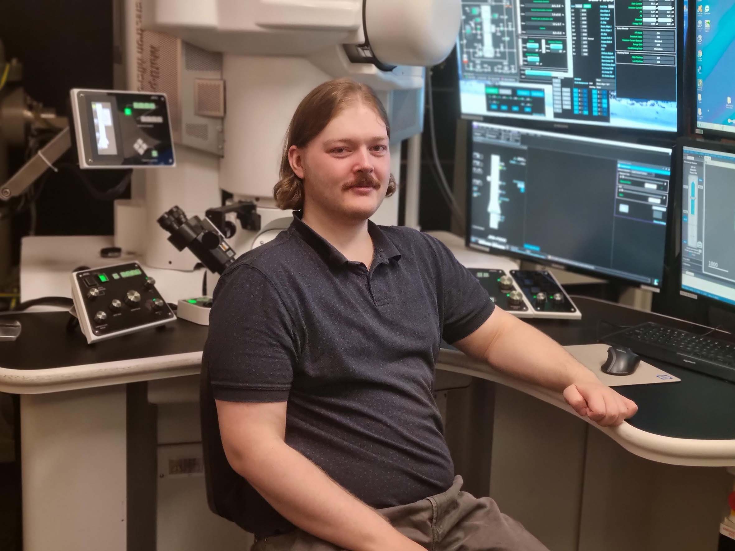
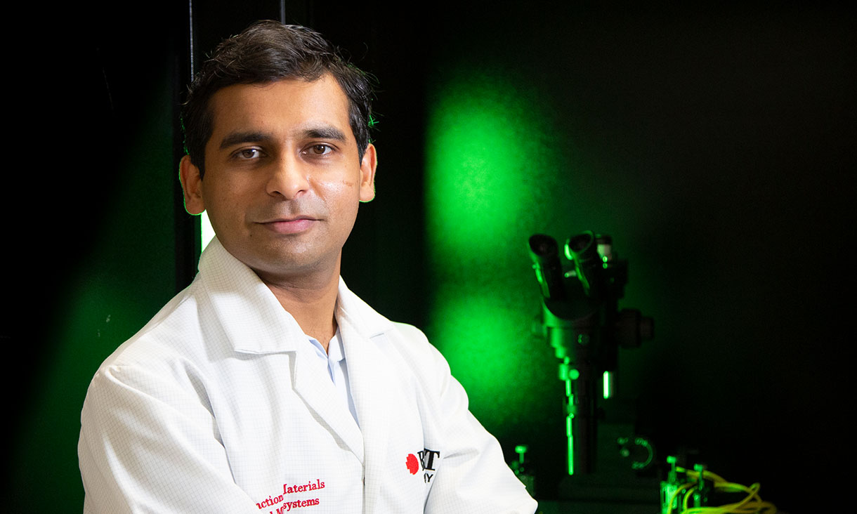
“This fluctuation of the solid metal surface between solid and liquid phases was completely unexpected,” says lead author Caiden Parker, “because the entire system was being kept at close to room-temperature conditions.”
“The liquid gallium ocean was over 200°C colder than the melting point of the Cu-Ga alloy. There would have seemed no possible reason for its surface to keep reverting back to liquid form,” says Caiden, who is a FLEET PhD candidate at RMIT.
In the video, the crystalline Cu-Ga alloy is identifiable from the regular lattice structure, which appears as diagonal stripes. The surrounding grey area is liquid gallium and not empty space.
Escape and recapture: A molecular view of the fluctuating boundary
“The outer layers of a solid metal alloy are surprisingly unstable when placed inside a liquid-metal environment, to the depth of several nanometres, fluctuating between crystalline and liquid states,” says team leader and corresponding author Prof Torben Daeneke (also at RMIT).
This crystal interface liquefaction, is observed at remarkably low temperatures (200°C below melting point of the solid), differentiating the observed liquefaction phenomenon from other processes such as surface pre-melting or conventional bulk melting.
The highly unstable crystal interface is observed in a variety of binary alloy systems and as such, the findings may impact the understanding of crystallisation and solidification processes in metallic systems and alloys more generally.
The crystal structure contains both ‘solute’ metal atoms (ie, copper) and ‘solvent’ metal atoms (gallium) thus forming a compound (CuGa2). The surface liquefaction process begins by losing some of the solvent metal atoms back into the surrounding liquid.
The researchers conducted molecular dynamic modelling in order to understand the observed surface fluidisation.
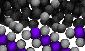
The modelling reveals that at the liquid-solid surface, some solvent (gallium) atoms will escape the solid structure due to that escape being energetically similar to staying in place.
Ie, a proportion of surface Ga atoms possess sufficient energy to escape the crystal lattice.
This ‘escape’ of atoms creates a vacancy at the surface, eventually creating an instability that leads to lattice collapse, causing the liquid-solid boundary to retreat inwards, into the solid.
Following this, the liquid becomes supersaturated in the solute (copper), forcing the surrounding liquid to re-bind with the crystal lattice. This causes the liquid-solid boundary to advance outwards again, back into the liquid.
The result is that the liquid-solid boundary oscillates backwards and forwards within a timespan of approximately half a second.
In the video of the molecular model, gallium atoms are represented in two colours: grey spheres represent gallium atoms that begin the modelled period being bound in the CuGa2 crystal lattice. Dark-grey spheres represent gallium atoms that begin the modelled period as moving freely in the surrounding liquid ocean.
The video shows a fraction of a nanosecond during the first phase of the process, when boundary shifts inwards as crystal-bound atoms escape to join the surrounding liquid.
As the model runs, grey atoms (ie, initially bound gallium atoms) escape the crystal lattice to float off into an ocean of dark grey (the surrounding liquid gallium). After a short while (a few hundred picoseconds), the purple atoms (ie, copper atoms) also begin to dislodge from the lattice.
Opportunities for further research and exciting future applications
“We hope this discovery will open new understanding of how metals behave, for creating new research opportunities, application in new alloy processes, solders, and improved additive manufacturing (3D printing) processes.
Crystallisation of alloys from a molten state is a fundamental metallurgic process, and the authors believe that the solid-liquid fluctuation of the crystal surface will be occurring every time crystallisation occurs.
“That’s why this is so exciting” says Torben. “The alloying process is so widespread, and so important in creating the materials that support modern industry….”
“Yet, no-one knew this was happening.”
“Now that we have discovered this fluctuation happening at the surface of solid alloys as they form, other metal chemistry researchers are going to want to explore this further.”
And with further improved fundamental understanding of the process of alloy crystallisation, it’s highly likely this newly discovered phenomenon will find an application.
The process of solidification in the synthesis of metal alloys is crucial, dictating the final physical, chemical and mechanical properties, all profoundly impacted by the final crystalline structure, size and shape.
“We can’t know yet what applications this might ultimately lead to,” says Caiden. “We don’t know whether someone will use this new understanding to synthesise improved alloys, or to reduce energy-use in alloy creation, or… who knows what!”
“That’s why fundamental science is so cool!”
The study
“Spontaneous Liquefaction of Solid Metal–Liquid Metal Interfaces in Colloidal Binary Alloys” was published in Advanced Science in April 2024. DOI: 10.1002/advs.202400147
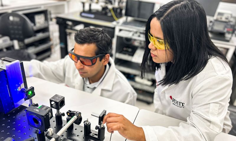
Tiny device mimics human vision and memory abilities
Researchers have created a small device that ‘sees’ and creates memories in a similar way to humans, in a promising step towards one day having applications that can make rapid, complex decisions such as in self-driving cars.
The neuromorphic invention is a single chip enabled by a sensing element, doped indium oxide, that is thousands of times thinner than a human hair and requires no external parts to operate.
RMIT University engineers led the work, with contributions from researchers at Deakin University and the University of Melbourne.
The team’s research demonstrates a working device that captures, processes and stores visual information. With precise engineering of the doped indium oxide, the device mimics a human eye’s ability to capture light, pre-packages and transmits information like an optical nerve, and stores and classifies it in a memory system like the way our brains can.
Collectively, these functions could enable ultra-fast decision making, the team says.
Team leader Professor Sumeet Walia said the new device can perform all necessary functions – sensing, creating and processing information, and retaining memories – rather than rely on external energy-intensive computation, which prevents real-time decision making.
“Performing all of these functions on one small device had proven to be a big challenge until now,” said Walia from the School of Engineering.
“We’ve made real-time decision making a possibility with our invention, because it doesn’t need to process large amounts of irrelevant data and it’s not being slowed down by data transfer to separate processors.”
What did the team achieve and how does the technology work?
The new device was able to demonstrate an ability to retain information for longer periods of time, compared to previously reported devices, without the need for frequent electrical signals to refresh the memory. This ability significantly reduces energy consumption and enhances the device’s performance.
Their findings and analysis are published in Advanced Functional Materials.
First author and RMIT PhD researcher Aishani Mazumder said the human brain used analog processing, which allowed it to process information quickly and efficiently using minimal energy.
“By contrast, digital processing is energy and carbon intensive, and inhibits rapid information gathering and processing,” she said.
“Neuromorphic vision systems are designed to use similar analog processing to the human brain, which can greatly reduce the amount of energy needed to perform complex visual tasks compared with today’s technologies.”
What are the potential applications?
The team used ultraviolet light as part of their experiments, and are working to expand this technology even further for visible and infrared light – with many possible applications such as bionic vision, autonomous operations in dangerous environments, shelf-life assessments of food and advanced forensics.
“Imagine a self-driving car that can see and recognise objects on the road in the same way that a human driver can or being able to able to rapidly detect and track space junk. This would be possible with neuromorphic vision technology.”
Walia said neuromorphic systems could adapt to new situations over time, becoming more efficient with more experience.
“Traditional computer vision systems – which cannot be miniaturised like neuromorphic technology – are typically programmed with specific rules and can’t adapt as easily,” he said.
“Neuromorphic robots have the potential to run autonomously for long periods, in dangerous situations where workers are exposed to possible cave-ins, explosions and toxic air.”
The human eye has a single retina that captures an entire image, which is then processed by the brain to identify objects, colours and other visual features.
The team’s device mimicked the retina’s capabilities by using single-element image sensors that capture, store and process visual information on one platform, Walia said.
“The human eye is exceptionally adept at responding to changes in the surrounding environment in a faster and much more efficient way than cameras and computers currently can,” he said.
“Taking inspiration from the eye, we have been working for several years on creating a camera that possesses similar abilities, through the process of neuromorphic engineering.”
Story first published: RMIT
‘Long duration persistent photocurrent in 3 nm thin doped indium oxide for integrated light sensing and in-sensor neuromorphic computation’, was published in Advanced Functional Materials in June 2023 (DOI: 10.1002/adfm.202303641)

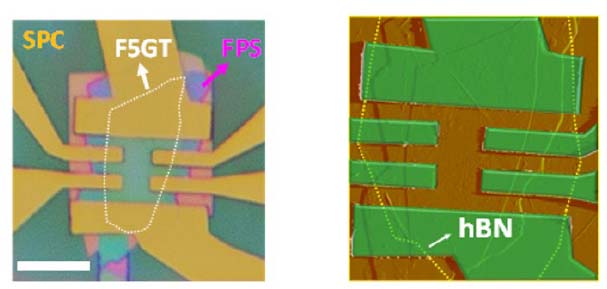
Manipulating interlayer magnetic coupling in vdW hetero-structures
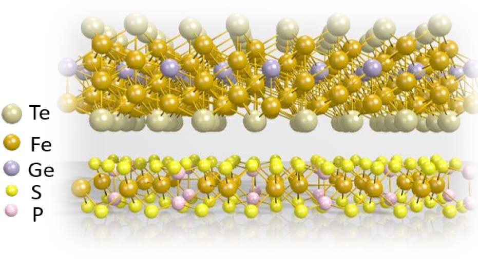
Electrical gate control in vdW heterostructures towards future spintronics
A FLEET RMIT-led international collaboration in 2022 observed, for the first time, electric gate-controlled exchange-bias effect in a van der Waals (vdW) hetero-structure, offering a promising platform for future energy-efficient, beyond-CMOS spintronics.
This new form of gate control would provide scalable, energy-efficient spin-orbit logic, which is very promising for beyond-CMOS devices in future low-energy electronic technologies.
It is the first successful significant manipulation of the exchange-bias effect (which is caused by interlayer magnetic coupling), which has been a significant goal in spintronics.
Electrical gate-manipulated exchange-bias effects in such magnetic hetero-structures enable scalable, energy-efficient spin-orbit logic, with the ‘blocking’ temperature of the exchange-bias effect effectively tuned via an electric gate.

This would allow the exchange-bias field to be turned ‘ON’ and ‘OFF’ in future spintronic transistors.
The FLEET-led collaboration of researchers at RMIT University and South China University of Technology confirmed for the first time the electric control of exchange-bias effect in a vdW heterostructure comprising antiferromagnetic (AFM) and ferromagnetic (FM) layers.
Such vdW magnetic hetero-structures provide an ideal platform for exploring interfacial magnetic-coupling mechanisms, boosting the development of vdW magnetic and spintronic devices.
The exchange-bias effect originates from the AFMFM interface coupling-induced unidirectional anisotropy. FLEET Research Fellow Dr Sultan Albarakati (RMIT)
“We decided it was time to utilise our experience in vdW hetero-structure-based nanodevices and gate control towards control magnetic properties in FM/ AFM bilayers,” says the study’s first author, FLEET Research Fellow Dr Sultan Albarakati (RMIT).
The team was also familiar with proton intercalation, which is an effective tool for modulating materials’ charge density.
The team’s expertise with magnetic materials informed materials chosen for the successful structure: a three-layer nanodevice featuring a ferromagnetic layer, antiferromagnetic layer and solid proton conductor.
The team then observed the shift of exchange-bias fields under different gate voltages.
“The blocking temperature of the exchange-bias effect can be effectively tuned via an electric gate. And more interestingly, the EB field can be switched ‘ON’ and ‘OFF’ repeatably under various gate voltages,” says co-author Dr Guolin Zheng (RMIT).
“Electric Control of Exchange Bias Effect in FePS3−Fe5GeTe2 van der Waals Heterostructures” was published in Nano Letters in August 2022. (DOI: 10.1021/acs.nanolett.2c01370)
Combining irradiation and lithography to engineer advanced conductive materials
Top-down patterning of topological surface and edge states using a focused ion beam for energy-efficient quantum electronics
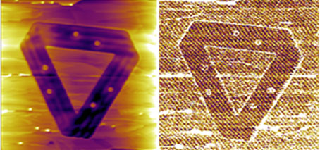
A new process developed to engineer nanoscale arrays of conducting channels for advanced scalable electronic circuitry unveils a useful pathway towards scalable topological electronics.
Using ion implantation and lithography, investigators created patterns of topological surface edge states on a topological material that made the surface edges conductive while the bulk layer beneath remained an insulator.
Low-energy ion implantation, neutron and X-ray reflectometry techniques at ANSTO supported the investigation, which was led by FLEET researchers at the University of Wollongong.
Investigators created patterns of topological surface edge states on antimony telluride (Sb2Te3 ), producing a 3D topological insulator with gapless, conductive surface edges and energy-gapped insulating bulk interior.
“The irradiation displaced atoms causing the transformation of the surface from a crystalline to a disordered glassy state,” explained FLEET Associate Investigator Dr David Cortie (ANSTO), who supervised lead author Abdulhakim Bake.
Ion beam implantation, commonly used to modify the properties of electronic materials by customised doping, has only recently been demonstrated on 2D materials or topological insulators.
In the work by Cortie’s team, lateral patterns were etched on thin flakes of the materials using a focused ion beam (FIB) instrument using low-energy gallium ions, such that the ions penetrate only a few nanometres into the material.
The researchers were able to combine ion beams and lithography to achieve dimensions smaller than 20 nanometres, with the shallow ion irradiation changing the surface’s atomic structure and electronic properties.
Importantly, the change in surface conductivity occurred at room temperature, suggesting a radical change in the electronic structure, confirmed by atomic force microscopy measurements by Dr Peggy Zhang, a Women in FLEET Fellow at UNSW.

X-ray diffraction and cross-sectional transmission electron microscopy confirmed the phase transition, and further experimentation with X-ray reflectometry and neutron reflectometry provided insights into the optimum ion beam dose to achieve the conversion.
Neutron reflectometry verified the thickness and morphology of the thin films and confirmed that the material remained the same chemical compound after the irradiation.
“The trick here is the judicious choice of the irradiation dose: if you under-irradiate, very little happens to the structure. But if you over-irradiate, you destroy the material via sputtering. We confirmed that we found the sweet spot for amorphisation,” said Dr Cortie.
Several different types of material were irradiated, including antimony telluride, bismuth telluride and bismuth selenide.
“In addition to standard FIB techniques, we also took advantage of the low energy implanter at ANSTO which is very flexible and can produce many different types of ions, including the noble gases and transition metal ions,” said Dr Cortie.
“The fields of amorphous and quasi-crystalline topological insulators are attracting a great deal of attention within the materials science sector. Our work provides some of the first experiments and should be useful to many people working in this field.”
“On the technological front, I also believe we have unveiled a very useful pathway towards scalable topological electronics using ion beams to define surface electronics.”
Story first published: ANSTO
Top-down patterning of topological surface and edge states using a focused ion beam was published in Nature Communications in March 2023 (DOI 10.1038/s41467-023-37102-x)