
Beating Boltzmann’s tyranny: Surpassing lower limit on computing energy consumption
Topological insulators can reduce transistor switching energy by a factor of four, defeating ‘Boltzmann's tyranny’, which puts a lower limit on operating voltage
A landmark theoretical FLEET study in 2021 confirms the potential for topological materials to substantially reduce the energy consumed by computing, defeating Boltzmann’s tyranny, a lower limit on operating energy.
The collaboration of researchers from three FLEET nodes showed that transistors based on topological insulators rather than conventional semiconductors could reduce the gate voltage by half, and the energy used by each transistor by a factor of four.
This overcomes the famous Boltzmann’s tyranny, which puts a lower limit on transistor switching energy.
The research discovered something surprising: a gate voltage applied to a topological insulator could create a barrier to electron flow that is larger than the voltage itself times the electron charge, a result previously thought impossible.
Transistors switch on and off based on application of a gate voltage, with the energy used to charge up the gate electrode lost each time each transistor switches. With literally billions of transistors turning on and off billions of times each second, this adds up to a lot of energy.
In conventional semiconductor transistors, a gate voltage shifts the semiconductor’s ‘bandgap’ (or the range of energies within which electrons are forbidden) to allow (the ‘on’ state) or block (the ‘off’ state) incoming electrons.
In an ideal transistor, 1 volt applied to the gate would move up the range of energies blocked by 1 electron-volt. But leakage ‘tyranny’ puts a lower limit on that switching energy.
With electrons’ energies inherently ‘smeared out’, there are always a few electrons with sufficiently-high energy to make it over the barrier. This ‘leakage’ current represents wasted energy.
To avoid wasted leakage current requires a minimum gate voltage that puts a lower limit on switching energy.
Named ‘Boltzmann’s tyranny’, after the scientist who first described the ‘smearing’ of the energies of particles by temperature, this limits how small the operating gate voltage can be for a transistor, no matter what material it is made of.
However, FLEET researchers wondered whether Boltzmann’s tyranny could be overcome in a new type of transistor using topological insulators, switched via an electric field rather than gate voltage.
Two-dimensional topological insulators can function as the ‘on’ state of a new type of transistor, with current carried by the conducting edges.
The conducting state of a such a material can be changed by an electric field, switching the material from dissipationless conduction (a topological insulator with a negative bandgap) to non-conduction (effectively, functioning as a regular semiconductor, with a positive bandgap blocking electron flow).
Crucially, the team found that, unlike a regular semiconductor, the increase in the bandgap in the topological insulator could be larger than the voltage applied to the gate, beating Boltzmann’s tyranny.
The next steps will be to confirm these findings in the laboratory, using candidate materials such as bismuthene, with FLEET working to synthesise these new materials, characterise them, and incorporate them into electronic devices.
Overcoming Boltzmann’s Tyranny in a Transistor via the Topological Quantum Field Effect was published in Nano Letters in March 2021 (DOI 10.1021/acs.nanolett.1c00378)

Combining irradiation and lithography to engineer advanced conductive materials
Top-down patterning of topological surface and edge states using a focused ion beam for energy-efficient quantum electronics
A new process developed to engineer nanoscale arrays of conducting channels for advanced scalable electronic circuitry unveils a useful pathway towards scalable topological electronics.
Using ion implantation and lithography, investigators created patterns of topological surface edge states on a topological material that made the surface edges conductive while the bulk layer beneath remained an insulator.
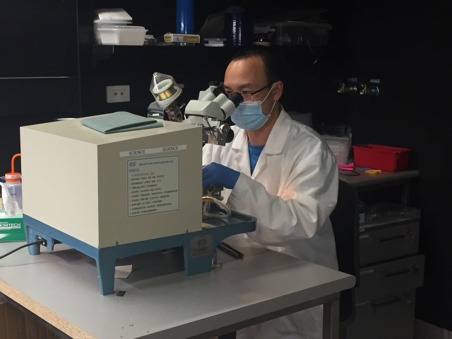
Low-energy ion implantation, neutron and X-ray reflectometry techniques at ANSTO supported the investigation, which was led by FLEET researchers at the University of Wollongong.
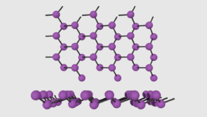
Investigators created patterns of topological surface edge states on antimony telluride (Sb2Te3 ), producing a 3D topological insulator with gapless, conductive surface edges and energy-gapped insulating bulk interior.
“The irradiation displaced atoms causing the transformation of the surface from a crystalline to a disordered glassy state,” explained FLEET Associate Investigator Dr David Cortie (ANSTO), who supervised lead author Abdulhakim Bake.
Ion beam implantation, commonly used to modify the properties of electronic materials by customised doping, has only recently been demonstrated on 2D materials or topological insulators.
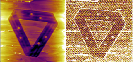
In the work by Cortie’s team, lateral patterns were etched on thin flakes of the materials using a focused ion beam (FIB) instrument using low-energy gallium ions, such that the ions penetrate only a few nanometres into the material.
The researchers were able to combine ion beams and lithography to achieve dimensions smaller than 20 nanometres, with the shallow ion irradiation changing the surface’s atomic structure and electronic properties.
Importantly, the change in surface conductivity occurred at room temperature, suggesting a radical change in the electronic structure, confirmed by atomic force microscopy measurements by Dr Peggy Zhang, a Women in FLEET Fellow at UNSW.

X-ray diffraction and cross-sectional transmission electron microscopy confirmed the phase transition, and further experimentation with X-ray reflectometry and neutron reflectometry provided insights into the optimum ion beam dose to achieve the conversion.
Neutron reflectometry verified the thickness and morphology of the thin films and confirmed that the material remained the same chemical compound after the irradiation.
“The trick here is the judicious choice of the irradiation dose: if you under-irradiate, very little happens to the structure. But if you over-irradiate, you destroy the material via sputtering. We confirmed that we found the sweet spot for amorphisation,” said Dr Cortie.
Several different types of material were irradiated, including antimony telluride, bismuth telluride and bismuth selenide.
“In addition to standard FIB techniques, we also took advantage of the low energy implanter at ANSTO which is very flexible and can produce many different types of ions, including the noble gases and transition metal ions,” said Dr Cortie.
“The fields of amorphous and quasi-crystalline topological insulators are attracting a great deal of attention within the materials science sector. Our work provides some of the first experiments and should be useful to many people working in this field.”
“On the technological front, I also believe we have unveiled a very useful pathway towards scalable topological electronics using ion beams to define surface electronics.”
Story first published: ANSTO
Top-down patterning of topological surface and edge states using a focused ion beam was published in Nature Communications in March 2023 (DOI 10.1038/s41467-023-37102-x)

Listening to nanoscale atomic avalanches
Listening to ‘crackling’ noise of atoms shifting at nanoscale when materials are deformed towards proposed, future domain-wall electronics.
A 2023 UNSW-led FLEET study published in Nature Communications presented an exciting new way to listen to avalanches of atoms in crystals.
The nanoscale movement of atoms when materials deform leads to sound emission. This so-called crackling noise is a scale-invariant phenomenon found in various material systems as a response to external stimuli such as force or external fields.
Jerky material movements in the form of avalanches can span many orders of magnitude in size and follow universal scaling rules described by power laws. The concept was originally studied as Barkhausen noise in magnetic materials and now is used in diverse fields from earthquake research and building materials monitoring to fundamental research involving phase transitions and neural networks.
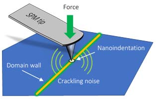
The new method for measuring nanoscale crackling noise developed by UNSW and University of Cambridge researchers is based on scanning probe microscope (SPM) nanoindentation (see figure).
“Our method allows us to study the crackling noise of individual nanoscale features in materials, such as domain walls in ferroelectrics,” says lead author Dr Cam Phu Nguyen. “The types of atom avalanches differ around these structures when the material deforms.”
One of the method’s most intriguing aspects is the fact that individual nanoscale features can be identified by imaging the material surface before indenting it. This differentiation enables new studies that were not possible previously. In a first application of the new technology, the UNSW researchers have used the method to investigate discontinuities in ordered materials, called domain walls.
“Domain walls have been the focus of our research for some time. They are highly attractive as building blocks for post–Moore’s Law electronics,” says author Prof Jan Seidel, also at UNSW. “We show that critical exponents for avalanches are altered at these nanoscale features, leading to a suppression of mixed-criticality, which is otherwise present in domains.”
From the perspective of applications and novel material functionalities, crackling noise microscopy presents a new opportunity for generating advanced knowledge about such features at the nanoscale. The study discusses experimental aspects of the method and provides a perspective on future research directions and applications.
The presented concept opens the possibility of investigating the crackling of individual nanoscale features in a wide range of other material systems.
Jerky material movements in the form of avalanches can span many orders of magnitude in size and follow universal scaling rules described by power laws. The concept was originally studied as Barkhausen noise in magnetic materials and now is used in diverse fields from earthquake research and building materials monitoring to fundamental research involving phase transitions and neural networks.
The new method for measuring nanoscale crackling noise developed by UNSW and University of Cambridge researchers is based on scanning probe microscope (SPM) nanoindentation (see figure). “Our method allows us to study the crackling noise of individual nanoscale features in materials, such as domain walls in ferroelectrics,” says lead author Dr Cam Phu Nguyen. “The types of atom avalanches differ around these structures when the material deforms.”
One of the method’s most intriguing aspects is the fact that individual nanoscale features can be identified by imaging the material surface before indenting it. This differentiation enables new studies that were not possible previously. In a first application of the new technology, the UNSW researchers have used the method to investigate discontinuities in ordered materials, called domain walls.
“Domain walls have been the focus of our research for some time. They are highly attractive as building blocks for post–Moore’s Law electronics,” says author Prof Jan Seidel, also at UNSW. “We show that critical exponents for avalanches are altered at these nanoscale features, leading to a suppression of mixed-criticality, which is otherwise present in domains.”
From the perspective of applications and novel material functionalities, crackling noise microscopy presents a new opportunity for generating advanced knowledge about such features at the nanoscale. The study discusses experimental aspects of the method and provides a perspective on future research directions and applications.
The presented concept opens the possibility of investigating the crackling of individual nanoscale features in a wide range of other material systems.
The paper Crackling noise microscopy was published in Nature Communications on 16 August 2023 (Cam-Phu Thi Nguyen, Peggy Schoenherr, Ekhard K. H. Salje, and Jan Seidel, DOI: 10.1038/s41467-023-40665-4).
Destroying conductivity in a kagome metal
Electrically-controlled superconductor-to-‘failed insulator’ transition and giant anomalous Hall effect in the kagome metal CsV3Sb5
An RMIT-led international collaboration published in 2023 uncovered, for the first time, a distinct disorder-driven bosonic superconductor–insulator transition.
The discovery outlines a global picture of the giant anomalous Hall effect and reveals its correlation with the unconventional charge density wave in a recently discovered kagome superconductor metal family, with potential applications in future ultra-low-energy electronics.
Superconductors, which can transmit electricity without energy dissipation, hold great promise for the development of future low-energy electronics technologies. They are already applied in diverse fields such as hover trains and medical magnetic resonance imaging (MRI) machines.
However, precisely how the superconductivity forms and works in many materials remains an unsolved issue and limits its applications. FLEET Research Fellow Dr Guolin Zheng (RMIT). “We wanted to see if we could achieve similar success as our trials using the proton gate technique in vdW spintronic devices, which effectively modulated similar carrier densities,” says first author, FLEET Research Fellow Dr Guolin Zheng (RMIT).
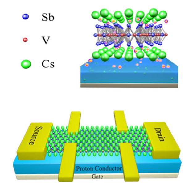
Recently, a new kagome superconductor family termed AV3Sb5has attracted intensive interest for their novel properties. (‘Kagome’ materials feature an unusual lattice named for a Japanese basket-weave pattern with corner-sharing triangles, and the A in AV3Sb5 refers to caesium, rubidium, or potassium.)
Although quantum phenomena accessible in AV3Sb5 materials provide ideal platforms for physics studies such as topology and strong correlations, the origin of these material’s giant anomalous Hall effect and superconductivity have remained unexplained, despite many recent investigations.
The FLEET-led collaboration of researchers at RMIT University and partner organisation the High Magnetic Field Laboratory (China) confirmed for the first time the electric control of superconductivity and anomalous Hall effect (AHE) in the van der Waals (vdW) kagome metal CsV3Sb5.
The key was manipulating the giant AHE via reversible proton intercalation.
“We wanted to see if we could achieve similar success as our trials using the proton gate technique in vdW spintronic devices, which effectively modulated similar carrier densities,” says first author, FLEET Research Fellow Dr Guolin Zheng (RMIT).
“The ability to tune the carrier density and the corresponding Fermi surfaces would play a vital role in understanding and manipulating these novel quantum states and would potentially realise some exotic quantum phase transitions.”
The team chose to test this theory on CsV3Sb5devices, easily designed and fabricated based on the FLEET team’s rich experience in this field. With thinner flakes, around 40 nanometres, the injection of the proton became quite easy, as well as being highly reversible. “Indeed, we have seldom met such a proton-friendly material!” says co-first author, FLEET Research Fellow Dr Cheng Tan (RMIT).
The unique coexistence of electronic correlations and band topology in AV3Sb5 materials allows investigation of intriguing transitions of these correlated states, such as superconductor-to-insulator transition, a quantum phase transition usually tuned by disorders, magnetic fields and electric gating.
The team’s further explorations of these potential quantum phase transitions met with success, but they were surprised to observe that the critical temperature of the phase shift decreased, showing a clear superconductor-to-insulator transition under increasing proton injection.
“Proton intercalation introduced disorder and suppressed both charge density wave and superconducting phase coherence,” says contributing-author A/Prof Lan Wang (also at RMIT). “And this gave rise to a superconductor–insulator transition associated with localised Cooper pairs and higher electrical resistance, dubbed a ‘failed insulator’”.
This discovery of a distinct, disorder-driven bosonic superconductor–insulator transition outlines a global picture of giant AHE and reveals its correlation with the well-known unconventional charge density wave in the CsV3Sb5 family. “This significant and electrically-controlled superconductor–insulator transition and anomalous Hall effect in kagome metals should inspire more investigations of the relevant intriguing physics, with promise for energy-saving nanoelectronic devices,” says Lan.
** “Electrically controlled superconductor-tofailed insulator transition and giant anomalous Hall effect in kagome metal CsV3Sb5 nanoflakes” was published in Nature Communications in February 2023. (DOI: 10.1038/s41467-023-36208-6)