
Top-down patterning of topological surface and edge states using a focused ion beam for energy-efficient quantum electronics
A new process developed to engineer nanoscale arrays of conducting channels for advanced scalable electronic circuitry unveils a useful pathway towards scalable topological electronics.
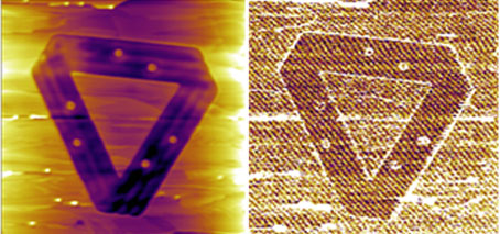
Using ion implantation and lithography, investigators created patterns of topological surface edge states on a topological material that made the surface edges conductive while the bulk layer beneath remained an insulator.
Low-energy ion implantation, neutron and X-ray reflectometry techniques at ANSTO supported the investigation, which was led by FLEET researchers at the University of Wollongong.
Investigators created patterns of topological surface edge states on antimony telluride (Sb2Te3 ), producing a 3D topological insulator with gapless, conductive surface edges and energy-gapped insulating bulk interior.

“The irradiation displaced atoms causing the transformation of the surface from a crystalline to a disordered glassy state,” explained FLEET Associate Investigator Dr David Cortie (ANSTO), who supervised lead author Abdulhakim Bake.
Ion beam implantation, commonly used to modify the properties of electronic materials by customised doping, has only recently been demonstrated on 2D materials or topological insulators.
In the work by Cortie’s team, lateral patterns were etched on thin flakes of the materials using a focused ion beam (FIB) instrument using low-energy gallium ions, such that the ions penetrate only a few nanometres into the material.
The researchers were able to combine ion beams and lithography to achieve dimensions smaller than 20 nanometres, with the shallow ion irradiation changing the surface’s atomic structure and electronic properties.
Importantly, the change in surface conductivity occurred at room temperature, suggesting a radical change in the electronic structure, confirmed by atomic force microscopy measurements by Dr Peggy Zhang, a Women in FLEET Fellow at UNSW.
X-ray diffraction and cross-sectional transmission electron microscopy confirmed the phase transition, and further experimentation with X-ray reflectometry and neutron reflectometry provided insights into the optimum ion beam dose to achieve the conversion.
Neutron reflectometry verified the thickness and morphology of the thin films and confirmed that the material remained the same chemical compound after the irradiation.
“The trick here is the judicious choice of the irradiation dose: if you under-irradiate, very little happens to the structure. But if you over-irradiate, you destroy the material via sputtering. We confirmed that we found the sweet spot for amorphisation,” said Dr Cortie.
Several different types of material were irradiated, including antimony telluride, bismuth telluride and bismuth selenide.
“In addition to standard FIB techniques, we also took advantage of the low energy implanter at ANSTO which is very flexible and can produce many different types of ions, including the noble gases and transition metal ions,” said Dr Cortie.
“The fields of amorphous and quasi-crystalline topological insulators are attracting a great deal of attention within the materials science sector. Our work provides some of the first experiments and should be useful to many people working in this field.”
“On the technological front, I also believe we have unveiled a very useful pathway towards scalable topological electronics using ion beams to define surface electronics.”
Story first published: ANSTO
Top-down patterning of topological surface and edge states using a focused ion beam was published in Nature Communications in March 2023 (DOI 10.1038/s41467-023-37102-x)