A/PROF LAN WANGLeader, Enabling technology B, RMIT
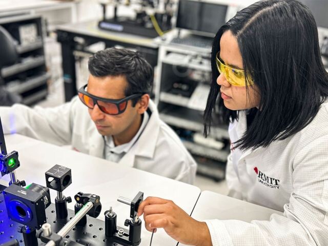
FLEET’s research sits at the very boundary of what is possible in condensed-matter physics. Thus, nanoscale fabrication of functioning devices have been key to the Centre’s ultimate success.
Specialised techniques are needed to integrate novel atomically-thin, two-dimensional (2D) materials into high-quality, high-performance nanodevices.
For example, successful development of functional topological transistors will require atomically-thin topological insulators to be integrated with electrical gates. And exciton-polariton condensate devices will require atomically-thin semiconductors to be integrated with optical cavities.
Nanodevice fabrication and characterisation link many of FLEET’s groups and nodes. Some groups bring expertise in device fabrication, while other groups are stronger in device characterisation.
FLEET brings Australian strength in microfabrication and nanofabrication together with world-leading expertise in van der Waals (vdW) hetero-structure fabrication to build the capacity for advanced atomically-thin device fabrication.
Case Studies
Nothing found.
Stories
Tiny device mimics human vision and memory abilities
Researchers have created a small device that ‘sees’ and creates memories in a similar way to humans, in a promising step towards one day having applications that can make rapid, complex decisions such as in self-driving cars.
Surfaces on the move: dynamic liquefaction
RMIT researchers have discovered that the liquid-solid boundary can fluctuate back and forth, with metallic atoms near the surface breaking free from their crystal lattice.

Manipulating interlayer magnetic coupling in vdW hetero-structures
A FLEET RMIT-led international collaboration in 2022 observed, for the first time, electric gate-controlled exchange-bias effect in a van der Waals (vdW) hetero-structure, offering a promising platform for future energy-efficient, beyond-CMOS spintronics.

Combining irradiation and lithography to engineer advanced conductive materials
A new process developed to engineer nanoscale arrays of conducting channels for advanced scalable electronic circuitry unveils a useful pathway towards scalable topological electronics.